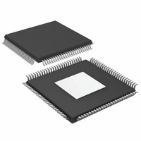
AD9779ABSVZRL Analog Devices Inc, AD9779ABSVZRL Datasheet - Page 7

AD9779ABSVZRL
Manufacturer Part Number
AD9779ABSVZRL
Description
IC,D/A CONVERTER,DUAL,16-BIT,CMOS,TQFP,100PIN
Manufacturer
Analog Devices Inc
Datasheet
1.AD9776ABSVZ.pdf
(60 pages)
Specifications of AD9779ABSVZRL
Design Resources
Interfacing ADL5370 to AD9779A Dual-Channel, 1 GSPS High Speed DAC (CN0016) Interfacing ADL5371 to AD9779A Dual-Channel, 1 GSPS High Speed DAC (CN0017) Interfacing ADL5372 to AD9779A Dual-Channel, 1 GSPS High Speed DAC (CN0018) Interfacing ADL5373 to AD9779A Dual-Channel, 1 GSPS High Speed DAC (CN0019) Interfacing ADL5374 to AD9779A Dual-Channel, 1 GSPS High Speed DAC (CN0020) Interfacing ADL5375 to AD9779A Dual-Channel, 1 GSPS High Speed DAC (CN0021)
Number Of Bits
16
Data Interface
Serial
Number Of Converters
2
Voltage Supply Source
Analog and Digital
Power Dissipation (max)
300mW
Operating Temperature
-40°C ~ 85°C
Mounting Type
Surface Mount
Package / Case
100-TQFP Exposed Pad, 100-eTQFP, 100-HTQFP, 100-VQFP
Lead Free Status / RoHS Status
Lead free / RoHS Compliant
For Use With
AD9779A-EBZ - BOARD EVALUATION FOR AD9779A
Settling Time
-
Lead Free Status / RoHS Status
Lead free / RoHS Compliant
Available stocks
Company
Part Number
Manufacturer
Quantity
Price
Company:
Part Number:
AD9779ABSVZRL
Manufacturer:
Analog Devices Inc
Quantity:
10 000
ABSOLUTE MAXIMUM RATINGS
Table 5.
Parameter
AVDD33, DVDD33
DVDD18, CVDD18
AGND
DGND
CGND
I120, VREF, IPTAT
OUT1_P, OUT1_N,
OUT2_P, OUT2_N,
AUX1_P, AUX1_N,
AUX2_P, AUX2_N
P1D<15> to P1D<0>,
P2D<15> to P2D<0>
DATACLK, TXENABLE
REFCLK+, REFCLK−
RESET, IRQ, PLL_LOCK,
SYNC_O+, SYNC_O−,
SYNC_I+, SYNC_I−,
CSB, SCLK, SDIO, SDO
Junction Temperature
Storage Temperature
Range
With Respect To
AGND, DGND,
CGND
AGND, DGND,
CGND
DGND, CGND
AGND, CGND
AGND, DGND
AGND
AGND
DGND
DGND
CGND
DGND
Rating
−0.3 V to +3.6 V
−0.3 V to +2.1 V
−0.3 V to +0.3 V
−0.3 V to +0.3 V
−0.3 V to +0.3 V
−0.3 V to
AVDD33 + 0.3 V
−1.0 V to
AVDD33 + 0.3 V
−0.3 V to
DVDD33 + 0.3 V
−0.3 V to
DVDD33 + 0.3 V
−0.3 V to
CVDD18 + 0.3 V
−0.3 V to
DVDD33 + 0.3 V
+125°C
−65°C to +150°C
Rev. A | Page 7 of 60
Stresses above those listed under Absolute Maximum Ratings
may cause permanent damage to the device. This is a stress
rating only; functional operation of the device at these or any
other conditions above those indicated in the operational
section of this specification is not implied. Exposure to absolute
maximum rating conditions for extended periods may affect
device reliability.
THERMAL RESISTANCE
For optimal thermal performance, the exposed paddle (EPAD)
should be soldered to the ground plane for the 100-lead,
thermally enhanced TQFP_EP package.
Typical θ
Airflow increases heat dissipation effectively reducing θ
Table 6. Thermal Resistance
Package Type
100-Lead TQFP_EP
ESD CAUTION
EPAD Soldered
EPAD Not Soldered
JA
and θ
JC
are specified for a 4-layer board in still air.
AD9776A/AD9778A/AD9779A
θ
19.1
27.4
JA
θ
12.4
JB
θ
7.1
JC
JA
.
Unit
°C/W
°C/W


