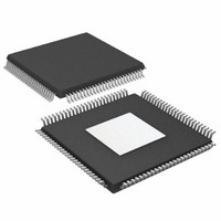
AD9779ABSVZRL Analog Devices Inc, AD9779ABSVZRL Datasheet - Page 49

AD9779ABSVZRL
Manufacturer Part Number
AD9779ABSVZRL
Description
IC,D/A CONVERTER,DUAL,16-BIT,CMOS,TQFP,100PIN
Manufacturer
Analog Devices Inc
Datasheet
1.AD9776ABSVZ.pdf
(60 pages)
Specifications of AD9779ABSVZRL
Design Resources
Interfacing ADL5370 to AD9779A Dual-Channel, 1 GSPS High Speed DAC (CN0016) Interfacing ADL5371 to AD9779A Dual-Channel, 1 GSPS High Speed DAC (CN0017) Interfacing ADL5372 to AD9779A Dual-Channel, 1 GSPS High Speed DAC (CN0018) Interfacing ADL5373 to AD9779A Dual-Channel, 1 GSPS High Speed DAC (CN0019) Interfacing ADL5374 to AD9779A Dual-Channel, 1 GSPS High Speed DAC (CN0020) Interfacing ADL5375 to AD9779A Dual-Channel, 1 GSPS High Speed DAC (CN0021)
Number Of Bits
16
Data Interface
Serial
Number Of Converters
2
Voltage Supply Source
Analog and Digital
Power Dissipation (max)
300mW
Operating Temperature
-40°C ~ 85°C
Mounting Type
Surface Mount
Package / Case
100-TQFP Exposed Pad, 100-eTQFP, 100-HTQFP, 100-VQFP
Lead Free Status / RoHS Status
Lead free / RoHS Compliant
For Use With
AD9779A-EBZ - BOARD EVALUATION FOR AD9779A
Settling Time
-
Lead Free Status / RoHS Status
Lead free / RoHS Compliant
Available stocks
Company
Part Number
Manufacturer
Quantity
Price
Company:
Part Number:
AD9779ABSVZRL
Manufacturer:
Analog Devices Inc
Quantity:
10 000
EVALUATION BOARD OPERATION
The AD9776A/AD9778A/AD9779A evaluation board is
designed to optimize the DAC performance and the speed of
the digital interface, yet remains user friendly. To operate the
board, the user needs a power source, a clock source, and a
digital data source. The user also needs a spectrum analyzer
or an oscilloscope to look at the DAC output. The diagram in
CLOCK IN
Figure 102. AD9776A/AD9778A/AD9779A Evaluation Board Showing All Connections
GENERATOR
PATTERN
DIGITAL
P4 DIGITAL INPUT CONNECTOR
DATACLK OUT
ADAPTER
CABLES
AUX33
S7 DCLKOUT
GENERATOR
CLOCK
DVDD18
Figure 101. Typical Test Setup
CLKIN
Rev. A | Page 49 of 60
EVALUATION
AD9779A
AD9776A/
AD9778A/
AD9779A
SPI PORT
BOARD
DVDD33
SPI PORT
J1 CLOCK IN
JP15
JP14
JP16
JP17
JP4
JP8
JP3
JP2
Figure 101 illustrates the test setup. A sine or square wave clock
works well as a clock source. The dc offset on the clock is not a
problem, because the clock is ac-coupled on the evaluation board
before the REFCLK inputs. All necessary connections to the
evaluation board are shown in more detail in Figure 102.
CVDD18
S5 OUTPUT 1
S6 OUTPUT 2
AVDD33
ADL537x
1.8V POWER SUPPLY
3.3V POWER SUPPLY
SPECTRUM
ANALYZER
MODULATOR
LOCAL OSC
5V SUPPLY
ANALOG
AD9776A/
AD9788A/
OUTPUT
DEVICES
AD9779A
INPUT
J2
AD9776A/AD9778A/AD9779A
+5V
GND


