AD9273BSVZ-25 Analog Devices Inc, AD9273BSVZ-25 Datasheet - Page 37
AD9273BSVZ-25
Manufacturer Part Number
AD9273BSVZ-25
Description
12Bit 25 MSPS Octal ADC
Manufacturer
Analog Devices Inc
Type
Crosspoint Switchr
Datasheet
1.AD9273BSVZ-25.pdf
(48 pages)
Specifications of AD9273BSVZ-25
Resolution (bits)
12 b
Sampling Rate (per Second)
25M
Data Interface
Serial
Voltage Supply Source
Single Supply
Voltage - Supply
1.7 V ~ 3.6 V
Operating Temperature
-40°C ~ 85°C
Mounting Type
Surface Mount
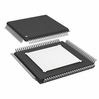
Package / Case
100-TQFP Exposed Pad, 100-eTQFP, 100-HTQFP, 100-VQFP
Lead Free Status / RoHS Status
Lead free / RoHS Compliant
Available stocks
Company
Part Number
Manufacturer
Quantity
Price
Company:

Part Number:
AD9273BSVZ-25
Manufacturer:
Analog Devices Inc
Quantity:
10 000


Power and Ground Recommendations
When connecting power to the AD9273, it is recommended
that two separate 1.8 V supplies be used: one for analog (AVDD)
and one for digital (DRVDD). If only one 1.8 V supply is
available, it should be routed to the AVDD1 first and then
tapped off and isolated with a ferrite bead or a filter choke
preceded by decoupling capacitors for the DRVDD. The user
should employ several decoupling capacitors on all supplies to
cover both high and low frequencies. These should be located
close to the point of entry at the PC board level and close to the
parts with minimal trace lengths.
A single PC board ground plane should be sufficient when
using the AD9273. With proper decoupling and smart parti-
tioning of the PC board’s analog, digital, and clock sections,
optimum performance can be achieved easily.
Exposed Paddle Thermal Heat Slug Recommendations
It is required that the exposed paddle on the underside of the
device be connected to a quiet analog ground to achieve the
best electrical and thermal performance of the AD9273. An
exposed continuous copper plane on the PCB should mate to
Rev. B | Page 37 of 48
the AD9273 exposed paddle, Pin 0. The copper plane should
have several vias to achieve the lowest possible resistive thermal
path for heat dissipation to flow through the bottom of the PCB.
These vias should be filled or plugged with nonconductive epoxy.
To maximize the coverage and adhesion between the device and
PCB, partition the continuous copper pad by overlaying a silk-
screen or solder mask to divide this into several uniform sections.
This ensures several tie points between the two during the reflow
process. Using one continuous plane with no partitions only
guarantees one tie point between the AD9273 and PCB. See
Figure 68 for a PCB layout example. For more detailed infor-
mation on packaging and for more PCB layout examples, see
the AN-772 Application Note.
SILKSCREEN PARTITION
PIN 1 INDICATOR
Figure 68. Typical PCB Layout
AD9273
Related parts for AD9273BSVZ-25
Image
Part Number
Description
Manufacturer
Datasheet
Request
R

Part Number:
Description:
±1.7g Dual-Axis IMEMS Accelerometer Evaluation Board
Manufacturer:
Analog Devices Inc
Datasheet:

Part Number:
Description:
Inertial Sensor Evaluation System
Manufacturer:
Analog Devices Inc
Datasheet:
Part Number:
Description:
Manufacturer:
Analog Devices Inc
Datasheet:
Part Number:
Description:
Manufacturer:
Analog Devices Inc
Datasheet:
Part Number:
Description:
Manufacturer:
Analog Devices Inc
Datasheet:
Part Number:
Description:
Manufacturer:
Analog Devices Inc
Datasheet:
Part Number:
Description:
Manufacturer:
Analog Devices Inc
Datasheet:
Part Number:
Description:
Manufacturer:
Analog Devices Inc
Datasheet:
Part Number:
Description:
Manufacturer:
Analog Devices Inc
Datasheet:
Part Number:
Description:
Manufacturer:
Analog Devices Inc
Datasheet:
Part Number:
Description:
Manufacturer:
Analog Devices Inc
Datasheet:
Part Number:
Description:
Manufacturer:
Analog Devices Inc
Datasheet:
Part Number:
Description:
Manufacturer:
Analog Devices Inc
Datasheet: