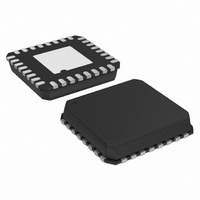
AD8376ACPZ-R7 Analog Devices Inc, AD8376ACPZ-R7 Datasheet - Page 6

AD8376ACPZ-R7
Manufacturer Part Number
AD8376ACPZ-R7
Description
If Cellular Dual DGA
Manufacturer
Analog Devices Inc
Datasheet
1.AD8376ACPZ-R7.pdf
(24 pages)
Specifications of AD8376ACPZ-R7
Design Resources
Using AD8376 to Drive Wide Bandwidth ADCs for High IF AC-Coupled Appls (CN0002) High Performance, Dual Channel IF Sampling Receiver (CN0140)
Amplifier Type
Variable Gain
Number Of Circuits
2
Output Type
Differential
Slew Rate
5000 V/µs
-3db Bandwidth
700MHz
Current - Input Bias
900nA
Current - Supply
250mA
Voltage - Supply, Single/dual (±)
4.5 V ~ 5.5 V
Operating Temperature
-40°C ~ 85°C
Mounting Type
Surface Mount
Package / Case
32-LFCSP
Lead Free Status / RoHS Status
Lead free / RoHS Compliant
Current - Output / Channel
-
Gain Bandwidth Product
-
Voltage - Input Offset
-
Lead Free Status / RoHS Status
Lead free / RoHS Compliant
Other names
AD8376ACPZ-R7TR
Available stocks
Company
Part Number
Manufacturer
Quantity
Price
Company:
Part Number:
AD8376ACPZ-R7
Manufacturer:
Maxim
Quantity:
26
Part Number:
AD8376ACPZ-R7
Manufacturer:
ADI/亚德诺
Quantity:
20 000
PIN CONFIGURATION AND FUNCTION DESCRIPTIONS
Table 4. Pin Function Descriptions
Pin No.
1
2
3
4
5
6
7
8
9
10
11
12
13, 20
14
15, 17
16, 18
19
21, 28
22
23, 25
24, 26
27
29
30
31
32
AD8376
A2
A3
A4
VCMA
VCMB
B4
B3
B2
B1
B0
IPB+
IPB−
GNDB
VCCB
OPB+
OPB−
ENBB
GNDA
ENBA
OPA−
OPA+
VCCA
IPA−
IPA+
A0
A1
Exposed Pad
Mnemonic
Description
MSB − 2 for the Gain Control Interface for Channel A.
MSB − 1 for the Gain Control Interface for Channel A.
MSB for the 5-Bit Gain Control Interface for Channel A.
Channel A Input Common-Mode Voltage. Typically bypassed to ground through capacitor.
Channel B Input Common-Mode Voltage. Typically bypassed to ground through capacitor.
MSB for the 5-Bit Gain Control Interface for Channel B.
MSB − 1 for the Gain Control Interface for Channel B.
MSB − 2 for the Gain Control Interface for Channel B.
LSB + 1 for the Gain Control Interface for Channel B.
LSB for the Gain Control Interface for Channel B.
Channel B Positive Input.
Channel B Negative Input.
Device Common (DC Ground) for Channel B.
Positive Supply Pin for Channel B. Should be bypassed to ground using suitable bypass capacitor.
Positive Output Pins (Open Collector) for Channel B. Require dc bias of +5 V nominal.
Negative Output Pins (Open Collector) for Channel B. Require dc bias of +5 V nominal.
Power Enable Pin for Channel B. Channel B is enabled with a logic high and disabled with a logic low.
Device Common (DC Ground) for Channel A.
Power Enable Pin for Channel A. Channel A is enabled with a logic high and disabled with a logic low.
Negative Output Pins (Open Collector) for Channel A. Require dc bias of +5 V nominal.
Positive Output Pins (Open Collector) for Channel A. Require dc bias of +5 V nominal.
Positive Supply Pins for Channel A. Should be bypassed to ground using suitable bypass capacitor.
Channel A Negative Input.
Channel A Positive Input.
LSB for the Gain Control Interface for Channel A.
LSB + 1 for the Gain Control Interface for Channel A.
Internally connected to ground. Solder to a low impedance ground plane.
NOTES
1. THE EXPOSED PAD IS INTERNALLY CONNECTED TO GROUND.
SOLDER TO A LOW IMPEDANCE GROUND PLANE.
VCMB
VCMA
A2
A3
A4
B4
B3
B2
1
2
3
4
5
6
7
8
Figure 3. 32-Lead LFCSP
Rev. A | Page 6 of 24
(Not to Scale)
PIN 1
INDICATOR
AD8376
TOP VIEW
24 OPA+
23 OPA–
22 ENBA
21 GNDA
20 GNDB
19 ENBB
18 OPB–
17 OPB+


