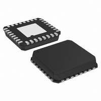
AD8376ACPZ-R7 Analog Devices Inc, AD8376ACPZ-R7 Datasheet - Page 13

AD8376ACPZ-R7
Manufacturer Part Number
AD8376ACPZ-R7
Description
If Cellular Dual DGA
Manufacturer
Analog Devices Inc
Datasheet
1.AD8376ACPZ-R7.pdf
(24 pages)
Specifications of AD8376ACPZ-R7
Design Resources
Using AD8376 to Drive Wide Bandwidth ADCs for High IF AC-Coupled Appls (CN0002) High Performance, Dual Channel IF Sampling Receiver (CN0140)
Amplifier Type
Variable Gain
Number Of Circuits
2
Output Type
Differential
Slew Rate
5000 V/µs
-3db Bandwidth
700MHz
Current - Input Bias
900nA
Current - Supply
250mA
Voltage - Supply, Single/dual (±)
4.5 V ~ 5.5 V
Operating Temperature
-40°C ~ 85°C
Mounting Type
Surface Mount
Package / Case
32-LFCSP
Lead Free Status / RoHS Status
Lead free / RoHS Compliant
Current - Output / Channel
-
Gain Bandwidth Product
-
Voltage - Input Offset
-
Lead Free Status / RoHS Status
Lead free / RoHS Compliant
Other names
AD8376ACPZ-R7TR
Available stocks
Company
Part Number
Manufacturer
Quantity
Price
Company:
Part Number:
AD8376ACPZ-R7
Manufacturer:
Maxim
Quantity:
26
Part Number:
AD8376ACPZ-R7
Manufacturer:
ADI/亚德诺
Quantity:
20 000
APPLICATIONS
BASIC CONNECTIONS
Figure 36 shows the basic connections for operating the
AD8376. A voltage between 4.5 V and 5.5 V should be applied
to the supply pins. Each supply pin should be decoupled with at
least one low inductance, surface-mount ceramic capacitor of
0.1 μF placed as close as possible to the device.
The outputs of the AD8376 are open collectors that need to be
pulled up to the positive supply with 1 μH RF chokes. The differ-
ential outputs are biased to the positive supply and require ac-
coupling capacitors, preferably 0.1 μF. Similarly, the input pins
are at bias voltages of about 2 V above ground and should be ac-
coupled as well. The ac-coupling capacitors and the RF chokes are
the principle limitations for operation at low frequencies.
To enable each channel of the AD8376, the ENBA or ENBB pin
must be pulled high. Taking ENBA or ENBB low puts the
channels of the AD8376 in sleep mode, reducing current
consumption to approximately 5 mA per channel at ambient.
SINGLE-ENDED-TO-DIFFERENTIAL CONVERSION
The AD8376 can be configured as a single-ended input to
differential output driver, as shown in Figure 34. A 150 Ω
resistor in parallel with the input impedance of input pin
provides an impedance matching of 50 Ω. The voltage gain and
the bandwidth of this configuration, using a 150 Ω load,
remains the same as when using a differential input.
Using a single-ended input decreases the power gain by 3 dB
and limits distortion cancellation. Consequently, the second-
order distortion is degraded. The third-order distortion remains
low to 200 MHz, as shown in Figure 35.
Rev. A | Page 13 of 24
–100
AC
50Ω
–60
–65
–70
–75
–80
–85
–90
–95
0
Figure 34. Single-Ended-to-Differential Conversion
Figure 35. Harmonic Distortion vs. Frequency of
150Ω
Single-Ended-to-Differential Conversion
37.5Ω
0.1µF
0.1µF
0.1µF
Featuring ½ of the AD8376
50
A0 TO A4
VCM
5
FREQUENCY (MHz)
AD8376
1/2
100
1µH
HD2
HD3
+5V
1µH
0.1µF
0.1µF
150
150Ω
AD8376
2
00


