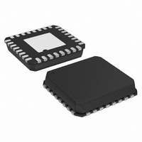
AD8376ACPZ-R7 Analog Devices Inc, AD8376ACPZ-R7 Datasheet - Page 18

AD8376ACPZ-R7
Manufacturer Part Number
AD8376ACPZ-R7
Description
If Cellular Dual DGA
Manufacturer
Analog Devices Inc
Datasheet
1.AD8376ACPZ-R7.pdf
(24 pages)
Specifications of AD8376ACPZ-R7
Design Resources
Using AD8376 to Drive Wide Bandwidth ADCs for High IF AC-Coupled Appls (CN0002) High Performance, Dual Channel IF Sampling Receiver (CN0140)
Amplifier Type
Variable Gain
Number Of Circuits
2
Output Type
Differential
Slew Rate
5000 V/µs
-3db Bandwidth
700MHz
Current - Input Bias
900nA
Current - Supply
250mA
Voltage - Supply, Single/dual (±)
4.5 V ~ 5.5 V
Operating Temperature
-40°C ~ 85°C
Mounting Type
Surface Mount
Package / Case
32-LFCSP
Lead Free Status / RoHS Status
Lead free / RoHS Compliant
Current - Output / Channel
-
Gain Bandwidth Product
-
Voltage - Input Offset
-
Lead Free Status / RoHS Status
Lead free / RoHS Compliant
Other names
AD8376ACPZ-R7TR
Available stocks
Company
Part Number
Manufacturer
Quantity
Price
Company:
Part Number:
AD8376ACPZ-R7
Manufacturer:
Maxim
Quantity:
26
Part Number:
AD8376ACPZ-R7
Manufacturer:
ADI/亚德诺
Quantity:
20 000
LAYOUT CONSIDERATIONS
Each amplifier has two output pins for each polarity, and they
are oriented in an alternating fashion. When designing the
board, care should be taken to minimize the parasitic capaci-
tance due to the routing that connects the corresponding
outputs together. A good practice is to avoid any ground or
power plane under this routing region and under the chokes to
minimize the parasitic capacitance.
CHARACTERIZATION TEST CIRCUITS
Differential-to-Differential Characterization
The S-parameter characterization for the AD8376 was
performed using a dedicated differential input to differential
output characterization board. Figure 45 shows the layout of the
characterization board. The board was designed for optimum
impedance matching into a 75 Ω system. Because both the
input and output impedances of the AD8376 are 150 Ω differ-
entially, 75 Ω impedance runs were used to match 75 Ω network
analyzer port impedances. On-board 1 μH inductors were used
for output biasing, and the output board traces were designed
for minimum capacitance.
AD8376
AC
75Ω
75Ω
Figure 43. Test Circuit for S-Parameters on Dedicated 75 Ω
75Ω TRACES
0.1µF
0.1µF
Differential-to-Differential Board
A0 TO A4
AD8376
5
1/2
AC
1µH
50Ω
L1
+5V
L2
1µH
T1
TC3-1T
0.1µF
0.1µF
75Ω TRACES
0.1µF
0.1µF
Figure 46. Test Circuit for Distortion, Gain, and Noise
C1
C2
A0 TO A4
AD8376
5
1/2
75Ω
75Ω
AC
Rev. A | Page 18 of 24
1µH
L1
+5V
L2
1µH
0.1µF
0.1µF
AC
C3
PAD LOSS = 11dB
C4
50Ω
62Ω
62Ω
R1
R2
Figure 45. Differential-to-Differential Characterization Board
T1
TC3-1T
Figure 44. Test Circuit for Time Domain Measurements
R4
25Ω
R3
25Ω
ETC1-1-13
0.1µF
0.1µF
A0 TO A4
AD8376
T2
5
Circuit Side Layout
1/2
50Ω
96Ω
+9V
96Ω
0.1µF
0.1µF
330Ω
330Ω
25Ω
25Ω
50Ω


