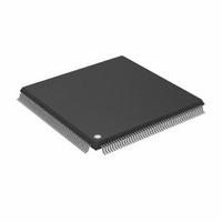
AD8151ASTZ Analog Devices Inc, AD8151ASTZ Datasheet - Page 17

AD8151ASTZ
Manufacturer Part Number
AD8151ASTZ
Description
IC,Telecom Switching Circuit,QFP,184PIN,PLASTIC
Manufacturer
Analog Devices Inc
Datasheet
1.AD8151AST.pdf
(40 pages)
Specifications of AD8151ASTZ
Function
Crosspoint Switch
Circuit
1 x 33:17
Voltage Supply Source
Dual Supply
Voltage - Supply, Single/dual (±)
±3 V ~ 5.25 V
Operating Temperature
0°C ~ 85°C
Mounting Type
Surface Mount
Package / Case
184-LQFP
Lead Free Status / RoHS Status
Lead free / RoHS Compliant
Available stocks
Company
Part Number
Manufacturer
Quantity
Price
Company:
Part Number:
AD8151ASTZ
Manufacturer:
Analog Devices Inc
Quantity:
10 000
Part Number:
AD8151ASTZ
Manufacturer:
ADI/亚德诺
Quantity:
20 000
CONTROL INTERFACE
D[0:6]
The AD8151 control interface receives and stores the desired
connection matrix for the 33 input and 17 output signal pairs.
The interface consists of 17 rows of double-rank 7-bit latches,
1 row for each output. The 7-bit data-word stored in each of
these latches indicates to which (if any) of the 33 inputs the
output is connected.
One output at a time can be preprogrammed by addressing the
output and writing the desired connection data into the first
rank of latches. This process can be repeated until each of the
desired output changes has been preprogrammed. All output
connections can then be programmed at once by passing the
data from the first rank of latches into the second rank. The
output connections always reflect the data programmed into the
second rank of latches and do not change until the first rank of
data is passed into the second rank.
If necessary for system verification, the data in the second rank
of latches can be read back from the control interface.
At any time, a reset pulse can be applied to the control interface
to globally reset the appropriate second rank data bits, disabling
all 17 signal output pairs. This feature can be used to avoid
output bus contention on system startup. The contents of the
first rank remain unchanged.
The control interface pins are connected via logic-level trans-
lators. These translators allow programming and readback of
the control interface using logic levels different from those in
the signal matrix.
WE
7
7
7
7
Figure 32. Control Interface (Simplified Schematic)
1 OF 17 DECODERS
A[0:4]
7
7
7
7
RANK 1
17 ROWS OF 7-BIT
16
2
0
1
UPDATE
LATCHES
RE
RANK 2
RESET
16
0
1
2
7
7
7
7
7
DECODERS
TO 17
SWITCH
MATRIX
7
7
7
7
1 OF 33
Rev. B | Page 17 of 40
×
33
33
33
33
33
To facilitate multiple chip address decoding, there is a chip-
select pin. All logic signals except the reset pulse are ignored
unless the chip select pin is active. The chip select pin disables
only the control logic interface and does not change the
operation of the signal matrix. The chip select pin does not
power down any of the latches, so any data programmed in the
latches is preserved.
All control pins are level-sensitive, not edge-triggered.
CONTROL PIN DESCRIPTION
A[4:0] Inputs
Output address pins. The binary encoded address applied to
these 5 input pins determines which one of the 17 outputs is
being programmed (or being read back). The most significant
bit (MSB) is A4.
D[6:0] Inputs/Outputs
Input configuration data pins. In write mode, the binary
encoded data applied to the D pins [6:0] determines which of
33 inputs is to be connected to the output specified with the
A pins [4:0]. The MSB is D5 and the least significant bit (LSB) is
D0. Bit D6 is the enable bit, setting the specified output signal
pair to an enabled state if D6 is logic high or disabled to a high
impedance state if D6 is logic low. In readback mode, the
D pins [6:0] are low impedance outputs, indicating the data-
word stored in the second rank for the output specified with the
A pins [4:0]. The readback drivers are designed to drive high
impedances only, so external drivers connected to the D
pins [6:0] should be disabled during readback mode.
WE Input
First Rank Write Enable. Forcing this pin to logic low allows the
data on the D pins [6:0] to be stored in the first rank latch for
the output specified by the A pins [4:0]. The WE pin must be
returned to a logic high state after a write cycle to avoid
overwriting the first rank data.
UPDATE Input
Second Rank Write Enable. Forcing this pin to logic low allows
the data stored in all 17 first rank latches to be transferred to the
second rank latches. The signal connection matrix is repro-
grammed when the second rank data is changed. This is a
global pin, transferring all 17 rows of data at once. It is not
necessary to program the address pins. It should be noted that
after the initial power-up of the device, the first rank data is
undefined. It may be desirable to preprogram all 17 outputs
before performing the first update cycle.
AD8151


