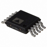
AD7791BRM Analog Devices Inc, AD7791BRM Datasheet - Page 3

AD7791BRM
Manufacturer Part Number
AD7791BRM
Description
Low Power 16-Bit SD ADC I.C.
Manufacturer
Analog Devices Inc
Datasheet
1.AD7791BRMZ-REEL.pdf
(20 pages)
Specifications of AD7791BRM
Rohs Status
RoHS non-compliant
Number Of Bits
24
Sampling Rate (per Second)
120
Data Interface
DSP, MICROWIRE™, QSPI™, Serial, SPI™
Number Of Converters
1
Power Dissipation (max)
230µW
Voltage Supply Source
Single Supply
Operating Temperature
-40°C ~ 105°C
Mounting Type
Surface Mount
Package / Case
10-TFSOP (0.118", 3.00mm Width)
Lead Free Status / RoHS Status
Contains lead / RoHS non-compliant
Available stocks
Company
Part Number
Manufacturer
Quantity
Price
Company:
Part Number:
AD7791BRM
Manufacturer:
AD
Quantity:
4 130
Company:
Part Number:
AD7791BRMZ
Manufacturer:
ADI
Quantity:
1 000
Company:
Part Number:
AD7791BRMZ
Manufacturer:
THAILAND
Quantity:
6 220
Part Number:
AD7791BRMZ
Manufacturer:
ADI/亚德诺
Quantity:
20 000
Company:
Part Number:
AD7791BRMZ-REEL
Manufacturer:
ADI
Quantity:
1 000
Part Number:
AD7791BRMZ-REEL
Manufacturer:
ADI/亚德诺
Quantity:
20 000
AD7791—SPECIFICATIONS
Table 1. (V
all specifications T
Parameter
ADC CHANNEL SPECIFICATION
ADC CHANNEL
ANALOG INPUTS
REFERENCE INPUT
1
2
3
4
Temperature Range –40°C to +105°C.
Specification is not production tested but is supported by characterization data at initial product release.
Full-scale error applies to both positive and negative full-scale and applies at the factory calibration conditions (V
FS[2:0] are the three bits used in the filter register to select the output word rate.
Output Update Rate
No Missing Codes
Resolution
Output Noise
Integral Nonlinearity
Offset Error
Offset Error Drift vs. Temperature
Full-Scale Error
Gain Drift vs. Temperature
Power Supply Rejection
Differential Input Voltage Ranges
Absolute AIN Voltage Limits
Analog Input Current
Absolute AIN Voltage Limits
Analog Input Current
Normal Mode Rejection
Common Mode Rejection
REFIN Voltage
Reference Voltage Range
Absolute REFIN Voltage Limits
Average Reference Input Current
Average Reference Input Current Drift
Average Input Current
Average Input Current Drift
Average Input Current
Average Input Current Drift
@ 50 Hz, 60 Hz
@ 50 Hz
@ 60 Hz
@DC
@ 50 Hz, 60 Hz
DD
= 2.5 V to 5.25 V; REFIN(+) = 2.5 V; REFIN(–) = GND; GND = 0 V; CDIV1 = CDIV0 = 0;
3
2
MIN
2
to T
2
2
2
MAX
2
2
, unless otherwise noted.)
2
1
AD7791B
9.5
120
24
19.5
1.1
±15
±3
±10
±10
±0.5
90
±REFIN
GND + 100 mV
V
±1
±5
GND – 30 mV
V
±400
±50
65
80
80
90
100
2.5
0.1
GND – 30 mV
V
0.5
±0.03
V
DD
DD
DD
DD
– 100 mV
+ 30 mV
+ 30 mV
Rev. 0 | Page 3 of 20
Unit
Hz min nom
Hz max nom
Bits min
Bits p-p
µV rms typ
ppm of FSR max
µV typ
nV/°C typ
µV typ
ppm/°C typ
dB min
V nom
V min
V max
nA max
pA/°C typ
V min
V max
nA/V typ
pA/V/°C typ
dB min
dB min
dB min
dB min
dB min
V nom
V min
V max
V min
V max
µA/V typ
nA/V/°C typ
Test Conditions/Comments
Update Rate ≤ 20 Hz
9.5 Hz Update Rate
3.5 ppm typ
100 dB typ, AIN = 1 V
REFIN = REFIN(+) – REFIN(–);
Buffered Mode of Operation
Buffered Mode of Operation
Unbuffered Mode of Operation
Unbuffered Mode of Operation
Input current varies with input voltage.
73 dB typ, 50 ± 1 Hz, 60 ± 1 Hz, FS[2:0] = 100
90 dB typ, 50 ± 1 Hz, FS[2:0] = 101
90 dB typ, 60 ± 1 Hz, FS[2:0] = 011
AIN = 1 V
100 dB typ, FS[2:0] = 100
50 ± 1 Hz (FS[2:0] = 101
REFIN = REFIN(+) – REFIN(–)
DD
= 4 V).
4
), 60 ± 1 Hz (FS[2:0] = 011
4
4
4
AD7791
4
4
)


