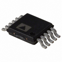
AD7791BRM Analog Devices Inc, AD7791BRM Datasheet - Page 18

AD7791BRM
Manufacturer Part Number
AD7791BRM
Description
Low Power 16-Bit SD ADC I.C.
Manufacturer
Analog Devices Inc
Datasheet
1.AD7791BRMZ-REEL.pdf
(20 pages)
Specifications of AD7791BRM
Rohs Status
RoHS non-compliant
Number Of Bits
24
Sampling Rate (per Second)
120
Data Interface
DSP, MICROWIRE™, QSPI™, Serial, SPI™
Number Of Converters
1
Power Dissipation (max)
230µW
Voltage Supply Source
Single Supply
Operating Temperature
-40°C ~ 105°C
Mounting Type
Surface Mount
Package / Case
10-TFSOP (0.118", 3.00mm Width)
Lead Free Status / RoHS Status
Contains lead / RoHS non-compliant
Available stocks
Company
Part Number
Manufacturer
Quantity
Price
Company:
Part Number:
AD7791BRM
Manufacturer:
AD
Quantity:
4 130
Company:
Part Number:
AD7791BRMZ
Manufacturer:
ADI
Quantity:
1 000
Company:
Part Number:
AD7791BRMZ
Manufacturer:
THAILAND
Quantity:
6 220
Part Number:
AD7791BRMZ
Manufacturer:
ADI/亚德诺
Quantity:
20 000
Company:
Part Number:
AD7791BRMZ-REEL
Manufacturer:
ADI
Quantity:
1 000
Part Number:
AD7791BRMZ-REEL
Manufacturer:
ADI/亚德诺
Quantity:
20 000
AD7791
CIRCUIT DESCRIPTION
ANALOG INPUT CHANNEL
The AD7791 has one differential analog input channel. This is
connected to the on-chip buffer amplifier when the device is
operated in buffered mode and directly to the modulator when
the device is operated in unbuffered mode. In buffered mode
(the BUF bit in the mode register is set to 1), the input channel
feeds into a high impedance input stage of the buffer amplifier.
Therefore, the input can tolerate significant source impedances
and is tailored for direct connection to external resistive-type
sensors such as strain gauges or resistance temperature detec-
tors (RTDs).
When BUF = 0, the part is operated in unbuffered mode. This
results in a higher analog input current. Note that this
unbuffered input path provides a dynamic load to the driving
source. Therefore, resistor/capacitor combinations on the input
pins can cause dc gain errors, depending on the output
impedance of the source that is driving the ADC input. Table 15
shows the allowable external resistance/capacitance values for
unbuffered mode such that no gain error at the 20-bit level is
introduced.
Table 15. External R-C Combination for No 20-Bit Gain Error
C (pF)
50
100
500
1000
5000
The absolute input voltage range in buffered mode is restricted
to a range between GND + 100 mV and V
must be taken in setting up the common-mode voltage so that
these limits are not exceeded. Otherwise, there will be degrada-
tion in linearity and noise performance.
The absolute input voltage in unbuffered mode includes the
range between GND – 30 mV and V
being unbuffered. The negative absolute input voltage limit does
allow the possibility of monitoring small true bipolar signals
with respect to GND.
BIPOLAR/UNIPOLAR CONFIGURATION
The analog input to the AD7791 can accept either unipolar or
bipolar input voltage ranges. A bipolar input range does not
imply that the part can tolerate negative voltages with respect to
system GND. Unipolar and bipolar signals on the AIN(+) input
are referenced to the voltage on the AIN(–) input. For example,
if AIN(–) is 2.5 V and the ADC is configured for unipolar
mode, the input voltage range on the AIN(+) pin is 2.5 V to 5 V.
R (Ω)
16.7K
9.6K
2.2K
1.1K
160
DD
+ 30 mV as a result of
DD
– 100 mV. Care
Rev. 0 | Page 18 of 20
If the ADC is configured for bipolar mode, the analog input
range on the AIN(+) input is 0 V to 5 V. The bipolar/unipolar
option is chosen by programming the B/U bit in the mode
register.
DATA OUTPUT CODING
When the ADC is configured for unipolar operation, the output
code is natural (straight) binary with a zero differential input
voltage resulting in a code of 00...00, a midscale voltage
resulting in a code of 100...000, and a full-scale input voltage
resulting in a code of 111...111. The output code for any analog
input voltage can be represented as
When the ADC is configured for bipolar operation, the output
code is offset binary with a negative full-scale voltage resulting
in a code of 000...000, a zero differential input voltage resulting
in a code of 100...000, and a positive full-scale input voltage
resulting in a code of 111...111. The output code for any analog
input voltage can be represented as
where AIN is the analog input voltage and N = 24.
REFERENCE INPUT
The AD7791 has a fully differential input capability for the
channel. The common-mode range for these differential inputs
is from GND to V
therefore, excessive R-C source impedances will introduce gain
errors. The reference voltage REFIN (REFIN(+) – REFIN(–)) is
2.5 V nominal, but the AD7791 is functional with reference
voltages from 0.1 V to V
(voltage or current) for the transducer on the analog input also
drives the reference voltage for the part, the effect of the low
frequency noise in the excitation source will be removed
because the application is ratiometric. If the AD7791 is used
in a nonratiometric application, a low noise reference should
be used.
Recommended 2.5 V reference voltage sources for the AD7791
include the ADR381 and ADR391, which are low noise, low
power references. In a system that operates from a 2.5 V power
supply, the reference voltage source will require some head-
room. In this case, a 2.048 V reference such as the ADR380 or
ADR390 can be used, requiring only 300 mV of headroom. Also
note that the reference inputs provide a high impedance,
dynamic load. Because the input impedance of each reference
input is dynamic, resistor/ capacitor combinations on these
inputs can cause dc gain errors, depending on the output
impedance of the source that is driving the reference inputs.
Code = 2
DD
. The reference input is unbuffered and,
Code = 2
DD
N – 1
. In applications where the excitation
× [(AIN/V
N
× (AIN/V
REF
REF
) + 1]
)


