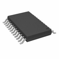
AD7492BRUZ Analog Devices Inc, AD7492BRUZ Datasheet - Page 9

AD7492BRUZ
Manufacturer Part Number
AD7492BRUZ
Description
IC,A/D CONVERTER,SINGLE,12-BIT,TSSOP,24PIN
Manufacturer
Analog Devices Inc
Datasheet
1.AD7492ARUZ.pdf
(16 pages)
Specifications of AD7492BRUZ
Number Of Bits
12
Sampling Rate (per Second)
1M
Data Interface
Parallel
Number Of Converters
1
Power Dissipation (max)
16.5mW
Voltage Supply Source
Analog and Digital
Operating Temperature
-40°C ~ 85°C
Mounting Type
Surface Mount
Package / Case
24-TSSOP (0.173", 4.40mm Width)
Lead Free Status / RoHS Status
Lead free / RoHS Compliant
For Use With
EVAL-AD7492CBZ - BOARD EVALUATION FOR AD7492
Lead Free Status / RoHS Status
Lead free / RoHS Compliant
CIRCUIT DESCRIPTION
CONVERTER OPERATION
The AD7492 is a 12-bit successive approximation analog-to-
digital converter based around a capacitive DAC. The AD7492
can convert analog input signals in the range 0 V to V
shows a very simplified schematic of the ADC. The Control
Logic, SAR, and the Capacitive DAC are used to add and sub-
tract fixed amounts of charge from the sampling capacitor to
bring the comparator back into a balanced condition.
–0.2
–0.4
–0.6
–0.8
–0.2
–0.4
–0.6
–0.8
CONTROL
0.8
0.6
0.4
0.2
0.8
0.6
0.4
0.2
–1
–1
1
0
1
0
INPUTS
0
0
V
REF
V
IN
512
512
CAPACITIVE
SWITCHES
1023
1023
DAC
SAR
CONTROL LOGIC
1534
1534
CODE
CODE
2045
2045
2556
2556
COMPARATOR
OUTPUT DATA
12-BIT PARALLEL
3067
3067
3578
3578
°
°
REF
4089
. Figure 2
4089
Figure 3 shows the ADC during its acquisition phase. SW2 is
closed and SW1 is in Position A. The comparator is held in a
balanced condition and the sampling capacitor acquires the
signal on V
Figure 4 shows the ADC during conversion. When conversion
starts, SW2 will open and SW1 will move to Position B, causing
the comparator to become unbalanced. The ADC then runs
through its successive approximation routine and brings the com-
parator back into a balanced condition. When the comparator is
rebalanced, the conversion result is available in the SAR register.
TYPICAL CONNECTION DIAGRAM
Figure 5 shows a typical connection diagram for the AD7492.
Conversion is initiated by a falling edge on CONVST. Once
CONVST goes low the BUSY signal goes high, and at the end
of conversion the falling edge of BUSY is used to activate an
Interrupt Service Routine. The CS and RD lines are then activated
in parallel to read the 12 data bits. The internal bandgap reference
voltage is 2.5 V, providing an analog input range of 0 V to 2.5 V,
making the AD7492 a unipolar A/D. A capacitor with a mini-
mum capacitance of 100 nF is needed at the output of the REF
OUT pin as it stabilizes the internal reference value. It is recom-
mended to perform a dummy conversion after power-up as the
first conversion result could be incorrect. This also ensures that
the part is in the correct mode of operation. The CONVST pin
should not be floating when power is applied as a rising edge on
CONVST might not wake up the part.
In Figure 5 the V
output voltage values being either 0 V or DV
applied to V
signals and the input logic signals. For example, if DV
supplied by a 5 V supply and V
output voltage levels would be either 0 V or 3 V. This feature
allows the AD7492 to interface to 3 V parts while still enabling
the A/D to process signals at 5 V supply.
AGND
AGND
V
V
IN
IN
IN
SW1
SW1
DRIVE
A
A
.
B
B
DRIVE
controls the voltage value of the output logic
pin is tied to DV
2k
2k
SW2
SW2
DRIVE
COMPARATOR
COMPARATOR
by a 3 V supply, the logic
DD
, which results in logic
CONTROL LOGIC
CONTROL LOGIC
DD
CAPACITIVE
CAPACITIVE
AD7492
. The voltage
DAC
DAC
DD
is


