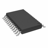
AD7492BRUZ Analog Devices Inc, AD7492BRUZ Datasheet - Page 12

AD7492BRUZ
Manufacturer Part Number
AD7492BRUZ
Description
IC,A/D CONVERTER,SINGLE,12-BIT,TSSOP,24PIN
Manufacturer
Analog Devices Inc
Datasheet
1.AD7492ARUZ.pdf
(16 pages)
Specifications of AD7492BRUZ
Number Of Bits
12
Sampling Rate (per Second)
1M
Data Interface
Parallel
Number Of Converters
1
Power Dissipation (max)
16.5mW
Voltage Supply Source
Analog and Digital
Operating Temperature
-40°C ~ 85°C
Mounting Type
Surface Mount
Package / Case
24-TSSOP (0.173", 4.40mm Width)
Lead Free Status / RoHS Status
Lead free / RoHS Compliant
For Use With
EVAL-AD7492CBZ - BOARD EVALUATION FOR AD7492
Lead Free Status / RoHS Status
Lead free / RoHS Compliant
AD7492
V
The V
drivers and the digital input circuitry. It is a separate supply
from AV
for the digital input/output interface is that the user can vary the
output high voltage, V
V
AV
powered from a 3 V supply. The ADC has better dynamic per-
formance at 5 V than at 3 V, so operating the part at 5 V, while
still being able to interface to 3 V parts, pushes the AD7492 to
the top bracket of high performance 12-bit A/Ds. Of course, the
ADC can have its V
and be powered from a 3 V or 5 V supply. The trigger levels are
V
The pins that are powered from V
RD, CONVST, and BUSY.
PS/FS PIN
As previously mentioned, the PS/FS pin is used to control the
type of power-down mode that the AD7492 can enter into if
operated in Mode 2. This pin can be hardwired either high or
low, or even controlled by another device. It is important to
note that toggling the PS/FS pin while in power-down mode will
not switch the part between partial sleep and full sleep modes.
To switch from one sleep mode to another, the AD7492 will have
to be powered up and the polarity of the PS/FS pin changed. It
can then be powered down to the required sleep mode.
POWER-UP
It is recommended that the user performs a dummy conversion
after power-up, as the first conversion result could be incorrect.
This also ensures that the parts is in the correct mode of opera-
tion. The recommended power-up sequence is as follows:
1 > GND
2 > V
3 > V
Power vs. Throughput
The two modes of operation for the AD7492 will produce dif-
ferent power versus throughput performances, Mode 1 and
Mode 2; see Operating Modes section of the data sheet for more
detailed descriptions of these modes. Mode 2 is the Sleep Mode
(Partial/Full) of the part and it achieves the optimum power
performance.
Mode 1
Figure 12 shows the AD7492 conversion sequence in Mode 1
using a throughput rate of 500 kSPS. At 5 V supply the current
consumption for the part when converting is 3 mA and the quies-
cent current is 1.8 mA. The conversion time of 880 ns contributes
6.6 mW to the overall power dissipation in the following way:
The contribution to the total power dissipated by the remaining
1.12 µs of the cycle is 5.04 mW.
Thus the power dissipated during each cycle is:
DRIVE
INL,
DRIVE
DD
from the V
DD
DRIVE
DRIVE
and DV
× 0.7 and V
DD
pin is used as the voltage supply to the digital output
and DV
(1.12 µs/2 µs) × (5 × 1.8 mA) = 5.04 mW
(880 ns/2 µs) × (5 × 3 mA) = 6.6 mW
DD
6.6 mW + 5.04 mW = 11.64 mW
4 > Digital Inputs
5 > V
DD
are using a 5 V supply, the V
DRIVE
DD
supply to the AD7492. For example, if
DRIVE
IN
OH
. The purpose of using a separate supply
, and the logic input levels, V
× 0.3 for the digital inputs.
and DV
DRIVE
DD
pins connected together
are DB0–DB11, CS,
DRIVE
pin can be
INH
and
Mode 2 (Full Sleep Mode)
Figure 13 shows the AD7492 conversion sequence in Mode 2,
Full Sleep mode, using a throughput rate of approximately
100 SPS. At 5 V supply the current consumption for the part
when converting is 3 mA, while the full sleep current is 1 µA
max. The power dissipated during this power-down is negligible
and thus not worth considering in the total power figure. During
the wake-up phase, the AD7492 will draw typically 1.8 mA. Over-
all power dissipated is:
Mode 2 (Partial Sleep Mode)
Figure 14 shows the AD7492 conversion sequence in Mode 2,
Partial Sleep mode, using a throughput rate of 1 kSPS. At 5 V
supply the current consumption for the part when converting is
3 mA, while the partial sleep current is 250 µA max. During the
wake-up phase, the AD7492 will draw typically 1.8 mA. Power
dissipated during wake-up and conversion is :
Power dissipated during power-down is:
Overall power dissipated is:
(880 ns/1 ms) × (5 × 3 mA) + (20 µs/1 ms) × (5 × 1.8 mA) =
(880 ns/10 ms) × (5 × 3 mA) + (500 µs/10 ms) × (5 × 1.8 mA)
CONVST
CONVST
BUSY
BUSY
CONVST
BUSY
(979 µs/1 ms) × (5 × 250 µA) = 1.22 mW
193.2 µW + 1.22 mW = 1.41 mW
t
t
WAKEUP
500 s
WAKEUP
20 s
t
CONVERT
880ns
t
t
= 451.32 µW
CONVERT
CONVERT
880ns
880ns
193.2 µW
10ms
1ms
2 s
t
t
QUIESCENT
QUIESCENT
t
QUIESCENT
979 s
1.12 s
9.5ms


