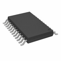
AD7492BRUZ Analog Devices Inc, AD7492BRUZ Datasheet - Page 13

AD7492BRUZ
Manufacturer Part Number
AD7492BRUZ
Description
IC,A/D CONVERTER,SINGLE,12-BIT,TSSOP,24PIN
Manufacturer
Analog Devices Inc
Datasheet
1.AD7492ARUZ.pdf
(16 pages)
Specifications of AD7492BRUZ
Number Of Bits
12
Sampling Rate (per Second)
1M
Data Interface
Parallel
Number Of Converters
1
Power Dissipation (max)
16.5mW
Voltage Supply Source
Analog and Digital
Operating Temperature
-40°C ~ 85°C
Mounting Type
Surface Mount
Package / Case
24-TSSOP (0.173", 4.40mm Width)
Lead Free Status / RoHS Status
Lead free / RoHS Compliant
For Use With
EVAL-AD7492CBZ - BOARD EVALUATION FOR AD7492
Lead Free Status / RoHS Status
Lead free / RoHS Compliant
Figure 15 to Figure 17 show a typical graphical representation
of Power versus Throughput for the AD7492 when in (a) Mode
1 @ 5 V and 3 V, (b) Mode 2 in full sleep mode @ 5 V and 3 V
and (c) Mode 2 in partial sleep mode @ 5 V and 3 V.
3.5
3.0
2.5
2.0
1.5
1.0
0.5
2.5
2.0
1.5
1.0
0.5
10
12
8
6
4
2
0
0
0
0
0
0
100
10
10
200
20
20
300
30
30
5V
THROUGHPUT – kHz
THROUGHPUT – kHz
THROUGHPUT – kHz
3V
400
40
40
3V
5V
5V
500
50
50
600
60
60
3V
700
70
70
800
80
80
900 1000
90
90
100
100
GROUNDING AND LAYOUT
The analog and digital power supplies are independent and
separately pinned out to minimize coupling between analog and
digital sections within the device. To complement the excellent
noise performance of the AD7492 it is imperative that care be
given to the PCB layout. Figure 18 shows a recommended
connection diagram for the AD7492.
All of the AD7492 ground pins should be soldered directly to a
ground plane to minimize series inductance. The AV
and V
digital ground planes. The REF OUT pin should be decoupled
to the analog ground plane with a minimum capacitor value of
100 nF. This capacitor helps to stabilize the internal reference
circuit. The large value capacitors will decouple low frequency
noise to analog ground, the small value capacitors will decouple
high frequency noise to digital ground. All digital circuitry power
pins should be decoupled to the digital ground plane. The use
of ground planes can physically separate sensitive analog com-
ponents from the noisy digital system. The two ground planes
should be joined in only one place and should not overlap so as
to minimize capacitive coupling between them. If the AD7492
is in a system where multiple devices require AGND to DGND
connections, the connection should still be made at one point
only, a star ground point, that should be established as close as
possible to the AD7492.
Noise can be minimized by applying some simple rules to the
PCB layout: analog signals should be kept away from digital
signals; fast switching signals like clocks should be shielded with
digital ground to avoid radiating noise to other sections of the
board and clock signals should never be run near the analog
inputs; avoid running digital lines under the device as these will
couple noise onto the die; the power supply lines to the AD7492
should use as large a trace as possible to provide a low imped-
ance path and reduce the effects of glitches on the power supply
line; avoid crossover of digital and analog signals and place
traces that are on opposite sides of the board at right angles
to each other.
Noise to the analog power line can be further reduced by use of
multiple decoupling capacitors as shown in Figure 18. Decou-
pling capacitors should be placed directly at the power inlet to
the PCB and also as close as possible to the power pins of the
AD7492. The same decoupling method should be used on other
ICs on the PCB, with the capacitor leads as short as possible to
minimize lead inductance.
2.5V
DRIVE
1nF
100nF
+
pins should be decoupled to both the analog and
+
10 F
10 F
1nF
+
DV
AGND
DGND
V
REF OUT
DRIVE
DD
AV
AD7492
DD
0.1 F
47 F
AD7492
+
DD
, DV
ANALOG
SUPPLY
5V
DD
,


