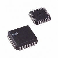
AD7248JPZ Analog Devices Inc, AD7248JPZ Datasheet - Page 5

AD7248JPZ
Manufacturer Part Number
AD7248JPZ
Description
12-BIT CMOS VOUT DACPORT
Manufacturer
Analog Devices Inc
Series
DACPORT®r
Datasheet
1.AD7245AARZ.pdf
(16 pages)
Specifications of AD7248JPZ
Settling Time
7µs
Number Of Bits
12
Data Interface
Parallel
Number Of Converters
1
Voltage Supply Source
Dual ±
Power Dissipation (max)
210mW
Operating Temperature
-40°C ~ 85°C
Mounting Type
Surface Mount
Package / Case
28-LCC (J-Lead)
Lead Free Status / RoHS Status
Lead free / RoHS Compliant
Available stocks
Company
Part Number
Manufacturer
Quantity
Price
Company:
Part Number:
AD7248JPZ
Manufacturer:
Analog Devices Inc
Quantity:
10 000
Pin
l
2
3
4
5
6–11
12
13–16 DB4–DB1
17
18
(MSB) DB11
REF OUT
AGND
DGND
DB10
R
DB9
DB8
DB7
DB6
DB5
Mnemonic Description
V
R
REF OUT
AGND
DB11
DB10–DB5 Data Bit 10 to Data Bit 5.
DGND
DB0
CS
V
OFS
SS
SS
OFS
10
11
12
1
2
3
4
5
6
7
8
9
DIP and SOIC
(NOT TO SCALE)
AD7245A
TOP VIEW
Negative Supply Voltage (0 V for single
supply operation).
Bipolar Offset Resistor. This provides
access to the on-chip application resistors
and allows different output voltage ranges.
Reference Output. The on-chip reference
is provided at this pin and is used when
configuring the part for bipolar outputs.
Analog Ground.
Data Bit 11. Most Significant Bit (MSB).
Digital Ground.
Data Bit 4 to Data Bit 1.
Data Bit 0. Least Significant Bit (LSB).
Chip Select Input (Active LOW). The
device is selected when this input is active.
24
23
22
21
20
19
18
17
16
15
14
13
CLR
LDAC
WR
CS
DB0 (LSB)
DB1
DB2
DB3
DB4
V
R
V
OUT
FB
DD
AD7245A PIN FUNCTION DESCRIPTIONS
AGND
DB11
DB10
DB9
DB8
DB7
NC = NO CONNECT
NC
AD7245A PIN CONFIGURATIONS
10
11
5
6
7
8
9
(DIP PIN NUMBERS)
12
4
13
3
(NOT TO SCALE)
14
PLCC
AD7245A
TOP VIEW
2
15
1
16
Pin
19
20
21
22
23
24
28
17
27
18
Mnemonic
WR
LDAC
CLR
V
R
V
26
DD
FB
OUT
25
24
23
22
21
20
19 DB1
CLR
LDAC
WR
NC
CS
DB0
Description
Write Input (Active LOW). This is used in
conjunction with CS to write data into the
input latch of the AD7245A.
Load DAC Input (Active LOW). This is
an asynchronous input which when active
transfers data from the input latch to the
DAC latch.
Clear Input (Active LOW). When this
input is active the contents of the DAC
latch are reset to all 0s.
Positive Supply Voltage.
Feedback Resistor. This allows access to
the amplifier’s feedback loop.
Output Voltage. Three different output
voltage ranges can be chosen: 0 V to 5 V,
0 V to 10 V or –5 V to +5 V.
AGND
DB11
DB10
DB9
DB8
DB7
NC
NC = NO CONNECT
10
11
7
5
6
8
9
AD7245A/AD7248A
12 13 14 15 16 17 18
4
(NOT TO SCALE)
3
AD7245A
TOP VIEW
2
LCCC
1 28 27 26
25
24
23
22
21
20
19
CLR
LDAC
WR
NC
CS
DB0
DB1


