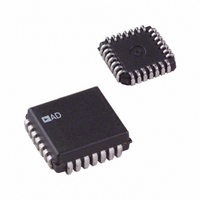
AD7248JPZ Analog Devices Inc, AD7248JPZ Datasheet - Page 12

AD7248JPZ
Manufacturer Part Number
AD7248JPZ
Description
12-BIT CMOS VOUT DACPORT
Manufacturer
Analog Devices Inc
Series
DACPORT®r
Datasheet
1.AD7245AARZ.pdf
(16 pages)
Specifications of AD7248JPZ
Settling Time
7µs
Number Of Bits
12
Data Interface
Parallel
Number Of Converters
1
Voltage Supply Source
Dual ±
Power Dissipation (max)
210mW
Operating Temperature
-40°C ~ 85°C
Mounting Type
Surface Mount
Package / Case
28-LCC (J-Lead)
Lead Free Status / RoHS Status
Lead free / RoHS Compliant
Available stocks
Company
Part Number
Manufacturer
Quantity
Price
Company:
Part Number:
AD7248JPZ
Manufacturer:
Analog Devices Inc
Quantity:
10 000
AD7245A/AD7248A
Since the tolerance value on the reference voltage of the AD7245A/
AD7248A is ± 0.2%, then the absolute value of I
± 0.2% from device to device for a fixed value of R1.
Because the input bias current of the AD7245A/AD7248A’s op
amp is only of the order of picoamps, its effect on the sink cur-
rent is negligible. Tying the R
effect even further and prevents noise pickup which could occur
if the R
The circuit of Figure 10 can be modified to provide a pro-
grammable current source to AGND or –V
dual supplies are required on the AD7245A/AD7248A). The
AD7245A/AD7248A is configured as before. The current through
R1 is mirrored with a current mirror circuit to provide the pro-
grammable source current (see CMOS DAC Application Guide,
Publication No. G872-30-10/84, for suitable current mirror
circuit). As before the absolute value of the source current will
be affected by the ±0.2% tolerance on V
mance of the current mirror will also affect the value of the
source current.
FUNCTION GENERATOR WITH PROGRAMMABLE
FREQUENCY
Figure 11 shows how the AD7245A/AD7248A with the AD537,
voltage-to-frequency converter and the AD639, trigonometric
function generator to provide a complete function generator
with programmable frequency. The circuit provides square wave,
triwave and sine wave outputs, each output of ± 10 V amplitude.
The AD7245A/AD7248A provides a programmable voltage to
the AD537 input. Since both the AD7245A/AD7248A and
AD537 are guaranteed monotonic, the output frequency will
always increase with increasing digital code. The AD537 pro-
vides a square wave output which is conditioned for ± 10 V by
amplifier A1. The AD537 also provides a differential triwave
output. This is conditioned by amplifiers A2 and A3 to provide the
±1.8 V triwave required at the input of the AD639. The triwave is
further scaled by amplifier A4 to provide a ±10 V output.
OFS
pin was left unconnected.
0.1 F
10
REF
OUT
AD7245A/
AD7248A
+
+15V
OFS
SQUARE
V
DGND
AGND
10 F
WAVE
DD
V
R
10V
OUT
R
V
OFS
input to R
FB
SS
+V
+
REF
S
. In this case the perfor-
20k
GND
DEC
FB
A1
AD537
SINK
input reduces this
SINK
+V
V
–V
O/P
15k
OS
(for –V
C
C
S
S
can vary by
4.7k
+15V
20k
+15V
SINK
33k
82k
,
+15V
680pF
C
F
A1, A2, A3, A4 – 2
10k
VR1
56k
56k
Adjusting the triwave applied to the AD639 adjust the distortion
performance of the sine wave output, (10 V in configuration
shown). Amplitude, offset and symmetry of the triwave can affect
the distortion. By adjusting these, via VR1 and VR2, an output
sine wave with harmonic distortion of better than –50 dB can be
achieved at low and intermediate frequencies.
Using the capacitor value shown in Figure 11 for C
the output frequency range is 0 to 100 kHz over the digital input
code range. The step size for frequency increments is 25 Hz.
The accuracy of the output frequency is limited to 8 or 9 bits by
the AD537, but is guaranteed monotonic to 12 bits.
MICROPROCESSOR INTERFACING—AD7245
AD7245A—8086 INTERFACE
Figure 12 shows the 8086 16-bit processor interfacing to the
AD7245A. In the setup shown in Figure 12, the double buffer-
ing feature of the DAC is not used and the LDAC input is tied
LOW. AD0–AD11 of the 16-bit data bus are connected to the
AD7245A data bus (DB0–DB11). The 12-bit word is written
to the AD7245A in one MOV instruction and the analog output
responds immediately. In this example the DAC address is
D000. A software routine for Figure 12 is given in Table V.
5.6k
5k
VR2
8086
AD15
4.12k
4.12k
A2
ALE
AD0
WR
A3
AD712
LINEAR CIRCUITRY OMITTED FOR CLARITY
LATCH
16-BIT
3.9k
3.9k
X1
X2
U1
U2
COM
Y2
AD639
ADDRESS/DATA BUS
ADDRESS BUS
22k
+V
–V
22k
UP
A4
Z1
Z2
W
S
S
ADDRESS
DECODE
+15V
–15V
–15V
TRI WAVE
SINE WAVE
10V
1V
CS
LDAC
WR
DB11
DB0
F
AD7245A
(i.e., 680 pF)


