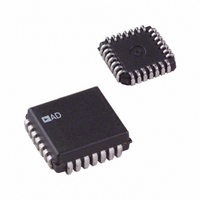
AD7248JPZ Analog Devices Inc, AD7248JPZ Datasheet - Page 3

AD7248JPZ
Manufacturer Part Number
AD7248JPZ
Description
12-BIT CMOS VOUT DACPORT
Manufacturer
Analog Devices Inc
Series
DACPORT®r
Datasheet
1.AD7245AARZ.pdf
(16 pages)
Specifications of AD7248JPZ
Settling Time
7µs
Number Of Bits
12
Data Interface
Parallel
Number Of Converters
1
Voltage Supply Source
Dual ±
Power Dissipation (max)
210mW
Operating Temperature
-40°C ~ 85°C
Mounting Type
Surface Mount
Package / Case
28-LCC (J-Lead)
Lead Free Status / RoHS Status
Lead free / RoHS Compliant
Available stocks
Company
Part Number
Manufacturer
Quantity
Price
Company:
Part Number:
AD7248JPZ
Manufacturer:
Analog Devices Inc
Quantity:
10 000
Parameter
t
t
t
t
t
t
t
t
NOTES
1
2
SWITCHING CHARACTERISTICS
CAUTION
ESD (electrostatic discharge) sensitive device. Electrostatic charges as high as 4000 V readily
accumulate on the human body and test equipment and can discharge without detection. Although
the AD7245A/AD7248A features proprietary ESD protection circuitry, permanent damage may
occur on devices subjected to high-energy electrostatic discharges. Therefore, proper ESD precautions
are recommended to avoid performance degradation or loss of functionality.
ABSOLUTE MAXIMUM RATINGS
V
V
V
AGND to DGND . . . . . . . . . . . . . . . . . . . . . . . . –0.3 V, V
Digital Input Voltage to DGND . . . . . . . –0.3 V, V
V
V
V
REF OUT
Power Dissipation (Any Package) to 75°C . . . . . . . . . 450 mW
Sample tested at 25°C to ensure compliance.
Power supply tolerance is ± 10%.
1
2
3
4
5
6
7
8
DD
DD
DD
OUT
OUT
OUT
(AD7245A Only)
@ 25°C
T
@ 25°C
T
@ 25°C
T
@ 25°C
T
@ 25°C
T
@ 25°C
T
@ 25°C
T
@ 25°C
T
Derates above 75°C by . . . . . . . . . . . . . . . . . . . . 6 mW/°C
MIN
MIN
MIN
MIN
MIN
MIN
MIN
MIN
to AGND . . . . . . . . . . . . . . . . . . . . . . . . –0.3 V to +17 V
to DGND . . . . . . . . . . . . . . . . . . . . . . . . –0.3 V to +17 V
to V
to AGND
to V
to V
to T
to T
to T
to T
to T
to T
to T
to T
SS
SS
DD
2
2
. . . . . . . . . . . . . . . . . . . . . . . . . . . –0.3 V to +34 V
MAX
MAX
MAX
MAX
MAX
MAX
MAX
MAX
to AGND . . . . . . . . . . . . . . . . . . . . . . . . 0 V, V
2
. . . . . . . . . . . . . . . . . . . . . . . . . . . . . . 0 V, 24 V
. . . . . . . . . . . . . . . . . . . . . . . . . . . . . –32 V, 0 V
2
. . . . . . . . . . . . . . . . . . . . . . . . . . . . V
A, B Versions
55
80
40
80
0
0
0
0
40
80
10
10
40
80
40
80
1
1
(V
DD
= +12 V to +15 V;
DD
+ 0.3 V
SS
, V
T Version
55
100
40
100
0
0
0
0
40
80
10
10
40
100
40
100
DD
DD
DD
Operating Temperature
Storage Temperature . . . . . . . . . . . . . . . . . . –65°C to +150°C
Lead Temperature (Soldering, 10 secs) . . . . . . . . . . . . . 300°C
NOTES
1
2
Stresses above those listed under Absolute Maximum Ratings may cause perma-
The output may be shorted to voltages in this range provided the power dissipation
2
nent damage to the device. This is a stress rating only; functional operation of the
device at these or any other conditions above those listed in the operational
sections of this specification is not implied. Exposure to absolute maximum rating
conditions for extended periods may affect device reliability.
of the package is not exceeded. V
80 mA.
V
Commercial (A, B Versions) . . . . . . . . . . . –40°C to +85°C
Extended (S Version) . . . . . . . . . . . . . . . –55°C to +125°C
SS
= 0 V to –12 V to –15 V;
Unit
ns typ
ns min
ns typ
ns min
ns min
ns min
ns min
ns min
ns typ
ns min
ns min
ns min
ns typ
ns min
ns typ
ns min
2
See Figures 5 and 7.)
Conditions
Chip Select Pulsewidth
Write Pulsewidth
Chip Select to Write Setup Time
Chip Select to Write Hold Time
Data Valid to Write Setup Time
Data Valid to Write Hold Time
Load DAC Pulsewidth
Clear Pulsewidth
AD7245A/AD7248A
OUT
WARNING!
short circuit current is typically
ESD SENSITIVE DEVICE


