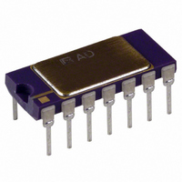
AD650AD Analog Devices Inc, AD650AD Datasheet - Page 7

AD650AD
Manufacturer Part Number
AD650AD
Description
IC,Voltage-to-Frequency Converter,BIPOLAR,DIP,14PIN
Manufacturer
Analog Devices Inc
Type
Volt to Freq & Freq to Voltr
Datasheet
1.AD650KNZ.pdf
(20 pages)
Specifications of AD650AD
Rohs Status
RoHS non-compliant
Frequency - Max
1MHz
Full Scale
±150ppm/°C
Linearity
±0.1%
Mounting Type
Through Hole
Package / Case
14-CDIP (0.300", 7.62mm)
Converter Function
VFC/FVC
Full Scale Frequency
1000
Power Supply Requirement
Dual
Single Supply Voltage (typ)
Not RequiredV
Single Supply Voltage (max)
Not RequiredV
Single Supply Voltage (min)
Not RequiredV
Dual Supply Voltage (min)
±9V
Dual Supply Voltage (max)
±18V
Operating Temperature (min)
-25C
Operating Temperature (max)
85C
Operating Temperature Classification
Commercial
Package Type
SBCDIP
Lead Free Status / Rohs Status
Not Compliant
Available stocks
Company
Part Number
Manufacturer
Quantity
Price
Part Number:
AD650AD
Manufacturer:
ADI/亚德诺
Quantity:
20 000
CIRCUIT OPERATION
UNIPOLAR CONFIGURATION
The AD650 is a charge balance voltage-to-frequency converter.
In the connection diagram shown in Figure 4, or the block
diagram of Figure 5, the input signal is converted into an
equivalent current by the input resistance R
exactly balanced by an internal feedback current delivered in
short, timed bursts from the switched 1 mA internal current
source. These bursts of current can be thought of as precisely
defined packets of charge. The required number of charge
packets, each producing one pulse of the output transistor,
depends upon the amplitude of the input signal. Because the
number of charge packets delivered per unit time is dependent
on the input signal amplitude, a linear voltage-to-frequency
transformation is accomplished. The frequency output is
furnished via an open collector transistor.
A more rigorous analysis demonstrates how the charge balance
voltage-to-frequency conversion takes place.
A block diagram of the device arranged as a V-to-F converter is
shown in Figure 5. The unit is comprised of an input integrator,
a current source and steering switch, a comparator, and a one
shot. When the output of the one shot is low, the current
steering switch S
amp; this is called the integration period. When the one shot
has been triggered and its output is high, the switch S
all the current to the summing junction of the op amp; this is
called the reset period. The two different states are shown in
Figure 6 and Figure 7 along with the various branch currents. It
should be noted that the output current from the op amp is the
same for either state, thus minimizing transients.
–15V
V
Figure 4. Connection Diagram for V/F Conversion, Positive Input Voltage
IN
R3
0.1µF
R
C
IN
INT
R1
C
OS
1
1
2
3
4
5
6
7
diverts all the current to the output of the op
FREQ
–V
S
OUT
SHOT
ONE
AMP
OP
AD650
IN
OUT
–V
S
S1
1mA
–0.6V
OFFSET
INPUT
TRIM
COMP
IN
14
13
12
11
10
. This current is
9
8
GROUND
DIGITAL
20kΩ
0.1µF
1µF
1
250kΩ
diverts
R2
ANALOG
GROUND
+15V
V
F
OUT
LOGIC
Rev. D | Page 7 of 20
+
–
–0.6
V
IN
R
I
IN
IN
INTEGRATOR
ΔV
AD650
RESET
+
–
+
–
V
V
t
S1
OS
IN
IN
Figure 8. Voltage Across C
Figure 7. Integrate Mode
C
Figure 5. Block Diagram
–V
1mA
R
R
I
I
INT
Figure 6. Reset Mode
IN
IN
IN
IN
S
1mA ± 20%
–0.6V
COMPARATOR
C
C
INT
INT
INTEGRATE
1mA – I
1mA – I
S1
S1
I
IN
1mA
–V
–V
T
1
S
S
IN
IN
t
1mA
1mA
SHOT
INT
OS
C
ONE
OS
FREQUENCY
OUTPUT
AD650
t
t


