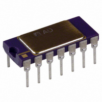
AD650AD Analog Devices Inc, AD650AD Datasheet - Page 3

AD650AD
Manufacturer Part Number
AD650AD
Description
IC,Voltage-to-Frequency Converter,BIPOLAR,DIP,14PIN
Manufacturer
Analog Devices Inc
Type
Volt to Freq & Freq to Voltr
Datasheet
1.AD650KNZ.pdf
(20 pages)
Specifications of AD650AD
Rohs Status
RoHS non-compliant
Frequency - Max
1MHz
Full Scale
±150ppm/°C
Linearity
±0.1%
Mounting Type
Through Hole
Package / Case
14-CDIP (0.300", 7.62mm)
Converter Function
VFC/FVC
Full Scale Frequency
1000
Power Supply Requirement
Dual
Single Supply Voltage (typ)
Not RequiredV
Single Supply Voltage (max)
Not RequiredV
Single Supply Voltage (min)
Not RequiredV
Dual Supply Voltage (min)
±9V
Dual Supply Voltage (max)
±18V
Operating Temperature (min)
-25C
Operating Temperature (max)
85C
Operating Temperature Classification
Commercial
Package Type
SBCDIP
Lead Free Status / Rohs Status
Not Compliant
Available stocks
Company
Part Number
Manufacturer
Quantity
Price
Part Number:
AD650AD
Manufacturer:
ADI/亚德诺
Quantity:
20 000
SPECIFICATIONS
T = 25°C, V
Table 1.
Model
DYNAMIC PERFORMANCE
BIPOLAR OFFSET CURRENT
DYNAMIC RESPONSE
ANALOG INPUT AMPLIFIER
COMPARATOR (F/V CONVERSION)
OPEN COLLECTOR OUTPUT
Full-Scale Frequency Range
Nonlinearity
Full-Scale Calibration Error
Activated by 1.24 kΩ Between
Maximum Settling Time for
Overload Recovery Time
(V/F CONVERSION)
(V/F CONVERSION)
Output Voltage in Logic 0
Output Leakage Current in Logic 1
Voltage Range
Current Input Range (Figure 4)
Voltage Input Range (Figure 12)
Differential Impedance
Common-Mode Impedance
Input Bias Current
Input Offset Voltage
Safe Input Voltage
Logic 0 Level
Logic 1 Level
Pulse Width Range
Input Impedance
f
f
f
f
100 kHz
1 MHz
vs. Supply
vs. Temperature
Pin 4 and Pin 5
Full-Scale Step Input
Step Input
Noninverting Input
Inverting Input
(Trimmable to Zero)
vs. Temperature (T
I
SINK
MAX
MAX
MAX
MAX
A, B, and S Grades
J and K Grades
≤ 8 mA, T
= 10 kHz
= 100 kHz
= 500 kHz
= 1 MHz
at 10 kHz
at 100 kHz
at 10 kHz
at 100 kHz
S
= ±15 V, unless otherwise noted.
1
3
5
MIN
to T
4
MIN
MAX
to T
2
MAX
)
0
Min
−0.015
0.45
1 pulse of new frequency plus 1 μs
1 pulse of new frequency plus 1 μs
0
−10
−V
0.1
0
S
AD650J/AD650A
Typ
0.002
0.005
0.02
0.1
± 5
± 10
±75
±150
0.5
2 MΩ||10 pF
1000 MΩ||10 pF
40
±8
±30
±V
250
S
Max
1
0.005
0.02
0.05
+0.015
±75
±150
0.55
+0.6
0
100
±20
±4
−1
+V
(0.3 × t
0.4
100
36
S
Rev. D | Page 3 of 20
OS
)
Min
−0.015
0.45
1 pulse of new frequency plus 1 μs
1 pulse of new frequency plus 1 μs
0
−10
−V
0
0.1
0
S
AD650K/AD650B
Typ
0.002
0.005
0.02
0.05
± 5
± 10
±75
±150
0.5
2 MΩ||10 pF
1000 MΩ||10 pF
40
±8
±V
250
S
Max
1
0.005
0.02
0.05
0.1
+0.015
±75
±150
0.55
+0.6
0
100
±20
±4
±30
−1
+V
(0.3 × t
0.4
100
36
S
OS
)
Min
−0.015
0.45
1 pulse of new frequency plus 1 μs
1 pulse of new frequency plus 1 μs
0
−10
−V
0
0.1
0
S
Typ
0.002
0.005
0.02
0.05
± 5
± 10
0.5
2 MΩ||10 pF
1000 MΩ||10 pF
40
±8
±V
250
AD650S
S
Max
1
0.005
0.02
0.05
0.1
+0.015
±75
±200
0.55
+0.6
0
100
±20
±4
±30
−1
+V
(0.3 × t
0.4
100
36
S
OS
AD650
)
Units
MHz
%
%
%
%
%
%
% of
FSR/V
ppm/°C
ppm/°C
ppm/°C
ppm/°C
mA
mA
V
nA
nA
mV
μV/°C
V
V
V
μs
kΩ
V
nA
V


