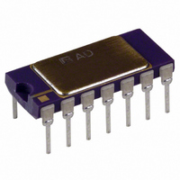
AD650AD Analog Devices Inc, AD650AD Datasheet

AD650AD
Specifications of AD650AD
Available stocks
Related parts for AD650AD
AD650AD Summary of contents
Page 1
... AD650 are specified for the commercial temperature range (0°C to 70°C). For industrial temperature range (−25°C to +85°C) applications, the AD650AD and AD650BD are offered in ceramic packages. The AD650SD is specified for the full −55°C to +125°C extended temperature range. ...
Page 2
AD650 TABLE OF CONTENTS Features .............................................................................................. 1 Functional Block Diagram .............................................................. 1 Product Description......................................................................... 1 Product Highlights ........................................................................... 1 Revision History ............................................................................... 2 Specifications..................................................................................... 3 Absolute Maximum Ratings............................................................ 5 ESD Caution.................................................................................. 5 Pin Configurations and Function Descriptions ........................... 6 Circuit ...
Page 3
SPECIFICATIONS T = 25° ±15 V, unless otherwise noted. S Table 1. Model Min DYNAMIC PERFORMANCE Full-Scale Frequency Range 1 Nonlinearity kHz MAX f = 100 kHz MAX f = 500 kHz MAX f = ...
Page 4
AD650 Model Min AMPLIFIER OUTPUT (F/V CONVERSION) Voltage Range (1500 Ω Min Load Resistance) 0 Source Current (750 Ω Max Load Resistance) 10 Capacitive Load (Without Oscillation) POWER SUPPLY Voltage, Rated Performance ±9 Quiescent Current TEMPERATURE RANGE Rated Performance N ...
Page 5
ABSOLUTE MAXIMUM RATINGS Parameter Total Supply Voltage Storage Temperature Range Differential Input Voltage Maximum Input Voltage Open Collector Output Voltage Above Digital GND Current Amplifier Short Circuit to Ground Comparator Input Voltage ESD CAUTION ESD (electrostatic discharge) sensitive device. Electrostatic ...
Page 6
AD650 PIN CONFIGURATIONS AND FUNCTION DESCRIPTIONS OUT + –IN AD650 3 12 BIBOLAR OFFSET TOP VIEW 4 11 CURRENT (Not to Scale) – ONE SHOT 6 CAPACITOR ...
Page 7
CIRCUIT OPERATION UNIPOLAR CONFIGURATION The AD650 is a charge balance voltage-to-frequency converter. In the connection diagram shown in Figure 4, or the block diagram of Figure 5, the input signal is converted into an equivalent current by the input resistance ...
Page 8
AD650 The positive input voltage develops a current (I charges the integrator capacitor charge builds up on INT C , the output voltage of the integrator ramps downward INT towards ground. When the integrator output voltage (Pin ...
Page 9
If the approximate amount of noise that appears then the value of C can be checked using the following NOISE INT inequality: − × × > − − ...
Page 10
AD650 BIPOLAR V/F Figure 11 shows how the internal bipolar current sink is used to provide a half-scale offset for a ±5 V signal range, while providing a 100 kHz maximum output frequency. The nominally 0.5 mA (±10%) offset current ...
Page 11
R3 C INT R1 1 AMP – –V S –15V 5 OUT 0.1µF FREQ ONE 6 SHOT Figure 12. Connection Diagram for V/F Conversion, Negative Input Voltage INT AMP ...
Page 12
AD650 DECOUPLING AND GROUNDING It is effective engineering practice to use bypass capacitors on the supply-voltage pins and to insert small-valued resistors (10 Ω to 100 Ω) in the supply lines to provide a measure of decoupling between the various ...
Page 13
Other circuit components do not directly influence the accuracy of the VFC over temperature changes as long as their actual values are not as different from the nominal value as to preclude operation. This includes the integration capacitor C in ...
Page 14
AD650 100k ACTUAL 50ppm IDEAL 100 10mV INPUT VOLTAGE Figure 16. Exaggerated Nonlinearity at 100 kHz Full Scale 1M ACTUAL VOLTAGE TO FREQUENCY TRANSFER RELATION 600ppm 1k 10mV INPUT VOLTAGE Figure 17. Exaggerated Nonlinearity at 1 MHz Full Scale 1k ...
Page 15
A second major difference is that the output only sinks the negative supply. There is no pulldown stage at the output other than the 1 mA current source used for the V-to-F conversion. The op amp sources ...
Page 16
AD650 APPLICATIONS DIFFERENTIAL VOLTAGE-TO-FREQUENCY CONVERSION The circuit in Figure 20 accepts a true floating differential input signal. The common-mode input can be in the range CM + −5 V with respect to analog ground. The signal ...
Page 17
PHASE-LOCKED LOOP F/V CONVERSION Although the F/V conversion technique shown in Figure 13 is quite accurate and uses only a few extra components very limited in terms of signal frequency response and carrier feed- through. If the carrier ...
Page 18
AD650 In signal recovery applications of a PLL, the desired output signal is the voltage applied to the oscillator. In these situations, a linear relationship between the input frequency and the output voltage is desired; the AD650 makes a superb ...
Page 19
OUTLINE DIMENSIONS PIN 1 0.210 (5.33) MAX 0.150 (3.81) 0.130 (3.30) 0.110 (2.79) 0.022 (0.56) 0.018 (0.46) 0.014 (0.36) 0.005 (0.13) MIN 0.080 (2.03) MAX 14 8 0.310 (7.87) 0.220 (5.59 PIN 1 0.100 (2.54) BSC 0.765 (19.43) ...
Page 20
... AD650KN 150 typ 0.1% max 1 AD650KNZ 150 typ 0.1% max AD650JP 150 typ 0.1% typ 1 AD650JPZ 150 typ 0.1% typ AD650AD 150 max 0.1% typ AD650BD 150 max 0.1% max AD650SD 200 max 0.1% max AD650SD/883B 200 max 0.1% max AD650ACHIPS Pb-free part. © ...


