AD5532ABC-2 Analog Devices Inc, AD5532ABC-2 Datasheet - Page 3
AD5532ABC-2
Manufacturer Part Number
AD5532ABC-2
Description
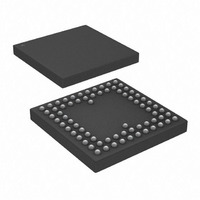
IC,Sample/Track-and-Hold Amplifier,32-CHANNEL,CMOS,BGA,74PIN,PLASTIC
Manufacturer
Analog Devices Inc
Specifications of AD5532ABC-2
Rohs Status
RoHS non-compliant
Settling Time
30µs
Number Of Bits
14
Data Interface
Serial
Number Of Converters
34
Voltage Supply Source
Analog and Digital
Power Dissipation (max)
623mW
Operating Temperature
-40°C ~ 85°C
Mounting Type
Surface Mount
Package / Case
74-CSPBGA
Number Of Channels
32
Resolution
14b
Conversion Rate
45KSPS
Interface Type
PARALLEL/SERIAL 3W
Single Supply Voltage (typ)
Not RequiredV
Dual Supply Voltage (typ)
±9/5/±12/5/±15/5V
Power Supply Requirement
Dual
Output Type
Voltage
Single Supply Voltage (min)
Not RequiredV
Single Supply Voltage (max)
Not RequiredV
Dual Supply Voltage (min)
-4.75/8/4.75V
Dual Supply Voltage (max)
±16.5/5.25V
Operating Temp Range
-40C to 85C
Operating Temperature Classification
Industrial
Mounting
Surface Mount
Pin Count
74
For Use With
EVAL-AD5532HSEBZ - BOARD EVAL FOR AD5532HSEVAL-AD5532EBZ - BOARD EVAL FOR AD5532
Lead Free Status / Rohs Status
Not Compliant
Available stocks
Company
Part Number
Manufacturer
Quantity
Price
Company:

Part Number:
AD5532ABC-2
Manufacturer:
AD
Quantity:
1 831
Company:
Part Number:
AD5532ABC-2
Manufacturer:
ADI
Quantity:
150
Company:
Part Number:
AD5532ABC-2
Manufacturer:
Analog Devices Inc
Quantity:
10 000


SPECIFICATIONS
V
REF_IN = 3 V; output range from V
Table 1.
Parameter
DAC DC PERFORMANCE
Full Scale Error
VOLTAGE REFERENCE
ANALOG OUTPUTS (V
Output Temperature Coefficient
ANALOG OUTPUT (OFFS_OUT)
DIGITAL INPUTS
DD
Resolution
Integral Nonlinearity (INL)
Differential Nonlinearity (DNL)
Offset
Gain
REF_IN
REF_OUT
DC Output Impedance
Output Range
Resistive Load
Capacitive Load
Short-Circuit Current
DC Power-Supply Rejection Ratio
DC Crosstalk
Output Temperature Coefficient
DC Output Impedance
Output Range
Output Current
Capacitive Load
Input Current
Input Low Voltage
Input High Voltage
Input Hysteresis (SCLK and CS Only)
= 8 V to 16.5 V, V
Nominal Input Voltage
Input Voltage Range
Input Current
Output Voltage
Output Impedance
Reference Temperature Coefficient
AD5532-1
AD5532-3
AD5532-5
AD5532-1
AD5532-3
AD5532-5
2
3
3
3, 5
3, 5
OUT
SS
3
3
= –4.75 V to –16.5 V; AV
0–31)
3
3
3
3, 4
3, 4
3
SS
+ 2 V to V
3
AD5532-1/-3/-5
14
±0.39
±1
90/170/250
3.52
±2
2.85/3.15
1
3
280
60
10
0.5
500
1
V
5
500
15
40
7
−70
−70
250
10
1.3
50 to REF_IN−12
10
100
±10
0.8
0.4
2.0
200
3.0
2.4
SS
+ 2/V
DD
CC
− 2 V. All outputs unloaded. All specifications T
= 4.75 V to 5.25 V; DV
DD
− 2
A Version
Rev. D | Page 3 of 20
AD5532-2 Only
14
±0.39
±1
180/350/500
7
±2
3.0
2.85/3.15
1
3
280
60
10
0.5
V
5
500
7
−70
−70
1800
10
1.3
50 to REF_IN−12
10
100
±10
0.8
0.4
2.4
2.0
200
SS
1
+ 2 /V
CC
DD
= 2.7 V to 5.25 V; AGND = DGND = DAC_GND = 0 V;
− 2
Unit
Bits
% of FSR max
LSB max
mV min/typ/max
typ
% of FSR max
V typ
V min/max
μA max
V typ
kΩ typ
ppm/°C typ
ppm/°C typ
Ω typ
Ω typ
kΩ typ
V min/max
kΩ min
pF max
nF max
nF max
mA typ
dB typ
dB typ
μV max
ppm/°C typ
kΩ typ
mV typ
μA max
pF max
μA max
V max
V max
V min
V min
mV typ
MIN
to T
MAX
Conditions/Comments
±0.15% typ
±0.5 LSB typ, monotonic
See Figure 8
< 1 nA typ
V
V
Source current
±5 μA typ
DV
DV
DV
DV
DD
SS
, unless otherwise noted.
CC
CC
CC
CC
= −15 V ±5%
= +15 V ±5%
= 5 V ±5%
= 3 V ±10%
= 5 V ±5%
= 3 V ±10%
AD5532
Related parts for AD5532ABC-2
Image
Part Number
Description
Manufacturer
Datasheet
Request
R

Part Number:
Description:
Cmos, 330 Mhz Triple 8-bit High Speed Video Dac
Manufacturer:
Analog Devices, Inc.
Datasheet:

Part Number:
Description:
±1.7g Dual-Axis IMEMS Accelerometer Evaluation Board
Manufacturer:
Analog Devices Inc
Datasheet:

Part Number:
Description:
Inertial Sensor Evaluation System
Manufacturer:
Analog Devices Inc
Datasheet:
Part Number:
Description:
Manufacturer:
Analog Devices Inc
Datasheet:
Part Number:
Description:
Manufacturer:
Analog Devices Inc
Datasheet:
Part Number:
Description:
Manufacturer:
Analog Devices Inc
Datasheet:
Part Number:
Description:
Manufacturer:
Analog Devices Inc
Datasheet:
Part Number:
Description:
Manufacturer:
Analog Devices Inc
Datasheet:
Part Number:
Description:
Manufacturer:
Analog Devices Inc
Datasheet:
Part Number:
Description:
Manufacturer:
Analog Devices Inc
Datasheet:
Part Number:
Description:
Manufacturer:
Analog Devices Inc
Datasheet:
Part Number:
Description:
Manufacturer:
Analog Devices Inc
Datasheet:
Part Number:
Description:
Manufacturer:
Analog Devices Inc
Datasheet: