AD5532ABC-2 Analog Devices Inc, AD5532ABC-2 Datasheet - Page 15
AD5532ABC-2
Manufacturer Part Number
AD5532ABC-2
Description
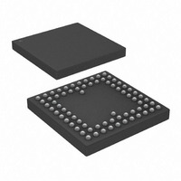
IC,Sample/Track-and-Hold Amplifier,32-CHANNEL,CMOS,BGA,74PIN,PLASTIC
Manufacturer
Analog Devices Inc
Specifications of AD5532ABC-2
Rohs Status
RoHS non-compliant
Settling Time
30µs
Number Of Bits
14
Data Interface
Serial
Number Of Converters
34
Voltage Supply Source
Analog and Digital
Power Dissipation (max)
623mW
Operating Temperature
-40°C ~ 85°C
Mounting Type
Surface Mount
Package / Case
74-CSPBGA
Number Of Channels
32
Resolution
14b
Conversion Rate
45KSPS
Interface Type
PARALLEL/SERIAL 3W
Single Supply Voltage (typ)
Not RequiredV
Dual Supply Voltage (typ)
±9/5/±12/5/±15/5V
Power Supply Requirement
Dual
Output Type
Voltage
Single Supply Voltage (min)
Not RequiredV
Single Supply Voltage (max)
Not RequiredV
Dual Supply Voltage (min)
-4.75/8/4.75V
Dual Supply Voltage (max)
±16.5/5.25V
Operating Temp Range
-40C to 85C
Operating Temperature Classification
Industrial
Mounting
Surface Mount
Pin Count
74
For Use With
EVAL-AD5532HSEBZ - BOARD EVAL FOR AD5532HSEVAL-AD5532EBZ - BOARD EVAL FOR AD5532
Lead Free Status / Rohs Status
Not Compliant
Available stocks
Company
Part Number
Manufacturer
Quantity
Price
Company:

Part Number:
AD5532ABC-2
Manufacturer:
AD
Quantity:
1 831
Company:
Part Number:
AD5532ABC-2
Manufacturer:
ADI
Quantity:
150
Company:
Part Number:
AD5532ABC-2
Manufacturer:
Analog Devices Inc
Quantity:
10 000


APPLICATION CIRCUITS
AD5533 in a Typical ATE System
The AD5533 infinite sample-and-hold is ideally suited for use
in automatic test equipment. Several ISHAs are required to
control pin drivers, comparators, active loads, and signal timing.
Traditionally, sample-and-hold devices with droop were used in
this application. These required refreshing to prevent the voltage
from drifting.
The AD5533 has several advantages: no refreshing is required,
there is no droop, pedestal error is eliminated, and there is no
need for extra filtering to remove glitches. Overall, a higher level
of integration is achieved in a smaller area, see Figure 13.
Typical Application Circuit
The AD5533 can be used to set up voltage levels on 32 channels
as shown in the circuit below. An AD780 provides the 3 V refer-
ence for the AD5533 and for the AD5541 16-bit DAC. A simple
3-wire interface is used to write to the AD5541. Because the
AD5541 has an output resistance of 6.25 kΩ (typ), the time taken
to charge/discharge the capacitance at the V
Hence an AD820 is used to buffer the DAC output. Note that it
is important to minimize noise on V
this circuit.
REV. A
SCLK
GENERATION
DIN
CS
AND INHIBIT
PATTERN
STORED
PERIOD
DELAY
TIMING
ISHAs
DATA
AND
AV
CC
Figure 14. Typical Application Circuit
Figure 13. AD5533 in an ATE System
AD5541*
AD780*
*ADDITIONAL PINS OMITTED FOR CLARITY
SYSTEM BUS
REF
V
OUT
FORMATTER
COMPARE
REGISTER
ISHA
ISHA
ISHA
AD820
ACTIVE
DRIVER
LOAD
V
COMPARATOR
DD
IN
ISHA
ISHA
and REFIN when laying out
V
OFFS_IN
OFFS_OUT
REFIN
MEASUREMENT
PARAMETRIC
IN
AV
SCLK DIN SYNC
AD5533*
CC
UNIT
IN
DV
ISHA
ISHA
Pin is significant.
CC
V
SS
SYSTEM BUS
DUT
V
OUT
0–31
–15–
POWER SUPPLY DECOUPLING
In any circuit where accuracy is important, careful consideration
of the power supply and ground return layout helps to ensure
the rated performance. The printed circuit board on which the
AD5533 is mounted should be designed so that the analog and
digital sections are separated and confined to certain areas of the
board. If the AD5533 is in a system where multiple devices
require an AGND-to-DGND connection, the connection should
be made at one point only. The star ground point should be
established as close as possible to the device. For supplies with
multiple pins (V
those pins together. The AD5533 should have ample supply
bypassing of 10 µF in parallel with 0.1 µF on each supply located
as close to the package as possible, ideally right up against the
device. The 10 µF capacitors are the tantalum bead type. The
0.1 µF capacitor should have low effective series resistance (ESR)
and effective series inductance (ESI), like the common ceramic
types that provide a low impedance path to ground at high frequen-
cies, to handle transient currents due to internal logic switching.
The power supply lines of the AD5533 should use as large a trace
as possible to provide low impedance paths and reduce the effects
of glitches on the power supply line. Fast switching signals, such as
clocks, should be shielded with digital ground to avoid radiating
noise to other parts of the board and should never be run near
the reference inputs. A ground line routed between the D
SCLK lines will help reduce crosstalk between them (not required
on a multilayer board as there will be a separate ground plane but
separating the lines will help).
Note it is essential to minimize noise on V
Particularly for optimum ISHA performance, the V
be kept noise-free. Depending on the noise performance of the
board, a noise filtering capacitor may be required on the V
If this capacitor is necessary, then for optimum throughput it may
be necessary to buffer the source which is driving V
over of digital and analog signals. Traces on opposite sides of the
board should run at right angles to each other. This reduces the
effects of feedthrough through the board. A microstrip technique is
by far the best but not always possible with a double-sided board.
In this technique, the component side of the board is dedicated
to ground plane while signal traces are placed on the solder side.
As is the case for all thin packages, care must be taken to avoid
flexing the package and to avoid a point load on the surface of
the package during the assembly process.
SS
, V
DD
, and AV
CC
), it is recommended to tie
IN
and REFIN lines.
AD5533
IN
. Avoid cross-
IN
line must
IN
IN
line.
and
Related parts for AD5532ABC-2
Image
Part Number
Description
Manufacturer
Datasheet
Request
R

Part Number:
Description:
Cmos, 330 Mhz Triple 8-bit High Speed Video Dac
Manufacturer:
Analog Devices, Inc.
Datasheet:

Part Number:
Description:
±1.7g Dual-Axis IMEMS Accelerometer Evaluation Board
Manufacturer:
Analog Devices Inc
Datasheet:

Part Number:
Description:
Inertial Sensor Evaluation System
Manufacturer:
Analog Devices Inc
Datasheet:
Part Number:
Description:
Manufacturer:
Analog Devices Inc
Datasheet:
Part Number:
Description:
Manufacturer:
Analog Devices Inc
Datasheet:
Part Number:
Description:
Manufacturer:
Analog Devices Inc
Datasheet:
Part Number:
Description:
Manufacturer:
Analog Devices Inc
Datasheet:
Part Number:
Description:
Manufacturer:
Analog Devices Inc
Datasheet:
Part Number:
Description:
Manufacturer:
Analog Devices Inc
Datasheet:
Part Number:
Description:
Manufacturer:
Analog Devices Inc
Datasheet:
Part Number:
Description:
Manufacturer:
Analog Devices Inc
Datasheet:
Part Number:
Description:
Manufacturer:
Analog Devices Inc
Datasheet:
Part Number:
Description:
Manufacturer:
Analog Devices Inc
Datasheet: