AD5532ABC-2 Analog Devices Inc, AD5532ABC-2 Datasheet - Page 14
AD5532ABC-2
Manufacturer Part Number
AD5532ABC-2
Description
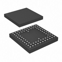
IC,Sample/Track-and-Hold Amplifier,32-CHANNEL,CMOS,BGA,74PIN,PLASTIC
Manufacturer
Analog Devices Inc
Specifications of AD5532ABC-2
Rohs Status
RoHS non-compliant
Settling Time
30µs
Number Of Bits
14
Data Interface
Serial
Number Of Converters
34
Voltage Supply Source
Analog and Digital
Power Dissipation (max)
623mW
Operating Temperature
-40°C ~ 85°C
Mounting Type
Surface Mount
Package / Case
74-CSPBGA
Number Of Channels
32
Resolution
14b
Conversion Rate
45KSPS
Interface Type
PARALLEL/SERIAL 3W
Single Supply Voltage (typ)
Not RequiredV
Dual Supply Voltage (typ)
±9/5/±12/5/±15/5V
Power Supply Requirement
Dual
Output Type
Voltage
Single Supply Voltage (min)
Not RequiredV
Single Supply Voltage (max)
Not RequiredV
Dual Supply Voltage (min)
-4.75/8/4.75V
Dual Supply Voltage (max)
±16.5/5.25V
Operating Temp Range
-40C to 85C
Operating Temperature Classification
Industrial
Mounting
Surface Mount
Pin Count
74
For Use With
EVAL-AD5532HSEBZ - BOARD EVAL FOR AD5532HSEVAL-AD5532EBZ - BOARD EVAL FOR AD5532
Lead Free Status / Rohs Status
Not Compliant
Available stocks
Company
Part Number
Manufacturer
Quantity
Price
Company:

Part Number:
AD5532ABC-2
Manufacturer:
AD
Quantity:
1 831
Company:
Part Number:
AD5532ABC-2
Manufacturer:
ADI
Quantity:
150
Company:
Part Number:
AD5532ABC-2
Manufacturer:
Analog Devices Inc
Quantity:
10 000


AD5533
MICROPROCESSOR INTERFACING
AD5533 to ADSP-21xx Interface
The ADSP-21xx family of DSPs are easily interfaced to the
AD5533 without the need for extra logic.
A data transfer is initiated by writing a word to the Tx Register
after the SPORT has been enabled. In a write sequence, data is
clocked out on each rising edge of the DSP’s serial clock and
clocked into the AD5533 on the falling edge of its SCLK. In
read back, 16 bits of data are clocked out of the AD5533 on each
rising edge of SCLK and clocked into the DSP on the rising edge of
SCLK. D
in the 16-bit Rx Register when using this configuration. The
SPORT Control Register should be set up as follows:
TFSW
INVRFS = INVTFS = 1, Active Low Frame Signal
DTYPE = 00, Right Justify Data
ISCLK = 1, Internal Serial Clock
TFSR
IRFS
ITFS
SLEN
SLEN
Figure 9 shows the connection diagram.
AD5533 to MC68HC11
The Serial Peripheral Interface (SPI) on the MC68HC11 is
configured for Master Mode (MSTR) = 1, Clock Polarity Bit
(CPOL) = 0, and the Clock Phase Bit (CPHA) = 1. The SPI is
configured by writing to the SPI Control Register (SPCR)—see
68HC11 User Manual. SCK of the 68HC11 drives the SCLK of
the AD5533, the MOSI output drives the serial data line (D
of the AD5533, and the MISO input is driven from D
SYNC signal is derived from a port line (PC7). When data is
being transmitted to the AD5533, the SYNC line is taken low
(PC7). Data appearing on the MOSI output is valid on the falling
edge of SCK. Serial data from the 68HC11 is transmitted in
8-bit bytes with only eight falling clock edges occurring in the
transmit cycle. Data is transmitted MSB first. To transmit 10 data
bits in ISHA Mode, it is important to left-justify the data in the
*ADDITIONAL PINS OMITTED FOR CLARITY
Figure 9. AD5533 to ADSP-2101/ADSP-2103 Interface
AD5533
IN
= RFSW = 1, Alternate Framing
= RFSR = 1, Frame Every Word
= 0, External Framing Signal
= 1, Internal Framing Signal
= 1001, 10-Bit Data-Words (ISHA Mode Write)
= 1111, 16-Bit Data-Words (Readback Mode)
is ignored. The valid 14 bits of data will be centered
*
SYNC
SCLK
D
OUT
D
IN
DR
TFS
RFS
DT
SCLK
ADSP-2101/
ADSP-2103*
OUT
. The
IN
)
–14–
SPDR Register. PC7 must be pulled low to start a transfer. It is
taken high and pulled low again before any further read/write cycles
can take place. A connection diagram is shown in Figure 10.
AD5533 to PIC16C6x/PIC16C7x
The PIC16C6x Synchronous Serial Port (SSP) is configured as an
SPI Master with the Clock Polarity Bit = 0. This is done by writing
to the Synchronous Serial Port Control Register (SSPCON). See
PIC16/PIC17 Microcontroller User Manual. In this example, I/O port
RA1 is being used to pulse SYNC and enable the serial port of
the AD5533. This microcontroller transfers only eight bits of data
during each serial transfer operation; therefore, two consecutive
read/write operations are needed for a 10-bit write and a 14-bit
read back. Figure 11 shows the connection diagram.
AD5533 to 8051
The AD5533 requires a clock synchronized to the serial data.
The 8051 serial interface must therefore be operated in Mode 0.
In this mode, serial data enters and exits through RxD and a
shift clock is output on TxD. Figure 12 shows how the 8051 is
connected to the AD5533. Because the AD5533 shifts data
out on the rising edge of the shift clock and latches data in on
the falling edge, the shift clock must be inverted. The AD5533
requires its data with the MSB first. Since the 8051 outputs
the LSB first, the transmit routine must take this into account.
*ADDITIONAL PINS OMITTED FOR CLARITY
*ADDITIONAL PINS OMITTED FOR CLARITY
*ADDITIONAL PINS OMITTED FOR CLARITY
AD5533
AD5533
AD5533
Figure 11. AD5533 to PIC16C6x/7x Interface
Figure 10. AD5533 to MC68HC11 Interface
Figure 12. AD5533 to 8051 Interface
*
*
*
SYNC
SCLK
SYNC
SYNC
SCLK
D
SCLK
D
D
OUT
OUT
D
OUT
D
D
IN
IN
IN
SCK/RC3
TxD
RxD
MISO
PC7
SCK
MOSI
SDO/RC5
SDI/RC4
RA1
P1.1
PIC16C6x/7x*
MC68HC11*
8051*
REV. A
Related parts for AD5532ABC-2
Image
Part Number
Description
Manufacturer
Datasheet
Request
R

Part Number:
Description:
Cmos, 330 Mhz Triple 8-bit High Speed Video Dac
Manufacturer:
Analog Devices, Inc.
Datasheet:

Part Number:
Description:
±1.7g Dual-Axis IMEMS Accelerometer Evaluation Board
Manufacturer:
Analog Devices Inc
Datasheet:

Part Number:
Description:
Inertial Sensor Evaluation System
Manufacturer:
Analog Devices Inc
Datasheet:
Part Number:
Description:
Manufacturer:
Analog Devices Inc
Datasheet:
Part Number:
Description:
Manufacturer:
Analog Devices Inc
Datasheet:
Part Number:
Description:
Manufacturer:
Analog Devices Inc
Datasheet:
Part Number:
Description:
Manufacturer:
Analog Devices Inc
Datasheet:
Part Number:
Description:
Manufacturer:
Analog Devices Inc
Datasheet:
Part Number:
Description:
Manufacturer:
Analog Devices Inc
Datasheet:
Part Number:
Description:
Manufacturer:
Analog Devices Inc
Datasheet:
Part Number:
Description:
Manufacturer:
Analog Devices Inc
Datasheet:
Part Number:
Description:
Manufacturer:
Analog Devices Inc
Datasheet:
Part Number:
Description:
Manufacturer:
Analog Devices Inc
Datasheet: