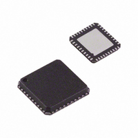
AD5412ACPZ-REEL7 Analog Devices Inc, AD5412ACPZ-REEL7 Datasheet - Page 8

AD5412ACPZ-REEL7
Manufacturer Part Number
AD5412ACPZ-REEL7
Description
12Bit 1V, I Out DAC
Manufacturer
Analog Devices Inc
Datasheet
1.AD5412ACPZ-REEL7.pdf
(40 pages)
Specifications of AD5412ACPZ-REEL7
Design Resources
Simplified 12-Bit Voltage and 4 mA-to-20 mA Output Solution Using AD5412 (CN0097)
Settling Time
25µs
Number Of Bits
12
Data Interface
MICROWIRE™, Serial, SPI™
Number Of Converters
1
Voltage Supply Source
Analog and Digital, Dual ±
Power Dissipation (max)
128mW
Operating Temperature
-40°C ~ 85°C
Mounting Type
Surface Mount
Package / Case
40-LFCSP
Number Of Channels
1
Resolution
12b
Conversion Rate
40KSPS
Interface Type
SER 3W SPI QSPI UW
Single Supply Voltage (typ)
12/15/18/24/28V
Architecture
R-2R
Power Supply Requirement
Single/Dual
Output Type
Current/Voltage
Single Supply Voltage (min)
10.8V
Single Supply Voltage (max)
40V
Dual Supply Voltage (min)
0/10.8V
Dual Supply Voltage (max)
-26.4/40V
Operating Temp Range
-40C to 85C
Operating Temperature Classification
Industrial
Mounting
Surface Mount
Pin Count
40
Lead Free Status / RoHS Status
Lead free / RoHS Compliant
Lead Free Status / RoHS Status
Lead free / RoHS Compliant
Other names
AD5412ACPZ-REEL7TR
Available stocks
Company
Part Number
Manufacturer
Quantity
Price
Company:
Part Number:
AD5412ACPZ-REEL7
Manufacturer:
Aptina
Quantity:
1 500
AD5412/AD5422
TIMING CHARACTERISTICS
AV
V
Table 4.
Parameter
WRITE MODE
READBACK MODE
DAISY-CHAIN MODE
1
2
3
4
Guaranteed by characterization; not production tested.
All input signals are specified with t
See Figure 2, Figure 3, and Figure 4.
C
t
t
t
t
t
t
t
t
t
t
t
t
t
t
t
t
t
t
t
t
t
t
t
t
t
t
t
t
t
t
OUT
1
2
3
4
5
5
6
7
8
9
10
11
12
13
14
15
16
17
18
19
20
21
22
23
24
25
26
27
28
29
L SDO
DD
: R
= capacitive load on SDO output.
= 10.8 V to 26.4 V, AV
LOAD
1, 2, 3
= 1 kΩ, C
L
= 200 pF, I
Limit at T
33
13
13
13
40
5
5
5
40
20
5
90
40
40
13
40
5
5
40
35
35
90
40
40
13
40
5
5
40
35
SS
= −26.4 V to −3 V/0 V, AV
R
= t
MIN
F
OUT
= 5 ns (10% to 90% of DV
, T
: R
MAX
LOAD
= 300 Ω; all specifications T
Unit
ns min
ns min
ns min
ns min
ns min
μs min
ns min
ns min
ns min
ns min
μs max
ns min
ns min
ns min
ns min
ns min
ns min
ns min
ns min
ns max
ns max
ns min
ns min
ns min
ns min
ns min
ns min
ns min
ns min
ns max
CC
) and timed from a voltage level of 1.2 V.
DD
+ |AV
Rev. C | Page 8 of 40
Description
SCLK cycle time
SCLK low time
SCLK high time
LATCH delay time
LATCH high time
LATCH high time (after a write to the control register)
Data setup time
Data hold time
LATCH low time
CLEAR pulse width
CLEAR activation time
SCLK cycle time
SCLK low time
SCLK high time
LATCH delay time
LATCH high time
Data setup time
Data hold time
LATCH low time
Serial output delay time (C
LATCH rising edge to SDO tristate (C
SCLK cycle time
SCLK low time
SCLK high time
LATCH delay time
LATCH high time
Data setup time
Data hold time
LATCH low time
Serial output delay time (C
SS
| < 52.8V, GND = 0 V, REFIN = +5 V external; DV
MIN
to T
MAX
, unless otherwise noted.
L SDO
L SDO
4
4
= 15 pF)
= 15 pF)
L SDO
4
= 15 pF)
CC
= 2.7 V to 5.5 V.


