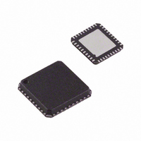
AD5412ACPZ-REEL7 Analog Devices Inc, AD5412ACPZ-REEL7 Datasheet - Page 7

AD5412ACPZ-REEL7
Manufacturer Part Number
AD5412ACPZ-REEL7
Description
12Bit 1V, I Out DAC
Manufacturer
Analog Devices Inc
Datasheet
1.AD5412ACPZ-REEL7.pdf
(40 pages)
Specifications of AD5412ACPZ-REEL7
Design Resources
Simplified 12-Bit Voltage and 4 mA-to-20 mA Output Solution Using AD5412 (CN0097)
Settling Time
25µs
Number Of Bits
12
Data Interface
MICROWIRE™, Serial, SPI™
Number Of Converters
1
Voltage Supply Source
Analog and Digital, Dual ±
Power Dissipation (max)
128mW
Operating Temperature
-40°C ~ 85°C
Mounting Type
Surface Mount
Package / Case
40-LFCSP
Number Of Channels
1
Resolution
12b
Conversion Rate
40KSPS
Interface Type
SER 3W SPI QSPI UW
Single Supply Voltage (typ)
12/15/18/24/28V
Architecture
R-2R
Power Supply Requirement
Single/Dual
Output Type
Current/Voltage
Single Supply Voltage (min)
10.8V
Single Supply Voltage (max)
40V
Dual Supply Voltage (min)
0/10.8V
Dual Supply Voltage (max)
-26.4/40V
Operating Temp Range
-40C to 85C
Operating Temperature Classification
Industrial
Mounting
Surface Mount
Pin Count
40
Lead Free Status / RoHS Status
Lead free / RoHS Compliant
Lead Free Status / RoHS Status
Lead free / RoHS Compliant
Other names
AD5412ACPZ-REEL7TR
Available stocks
Company
Part Number
Manufacturer
Quantity
Price
Company:
Part Number:
AD5412ACPZ-REEL7
Manufacturer:
Aptina
Quantity:
1 500
Parameter
1
2
3
4
5
AC PERFORMANCE CHARACTERISTICS
AV
V
Table 3.
Parameter
DYNAMIC PERFORMANCE
1
Temperature range: −40°C to +85°C; typical at +25°C.
When the AD5412/AD5422 is powered with AV
for the AD5412.
Guaranteed by design and characterization; not production tested.
For 0 mA to 20 mA and 0 mA to 24 mA ranges, INL is measured beginning from Code 256 for the AD5422 and Code 16 for the AD5412.
The on-chip reference is production trimmed and tested at 25°C and 85°C. It is characterized from −40°C to +85°C.
Guaranteed by characterization, not production tested.
OUT
AI
AI
DI
Power Dissipation
Voltage Output
Current Output
DD
DD
SS
CC
: R
Output Voltage Settling Time
Slew Rate
Power-On Glitch Energy
Digital-to-Analog Glitch Energy
Glitch Impulse Peak Amplitude
Digital Feedthrough
Output Noise (0.1 Hz to 10 Hz
Output Noise (100 kHz Bandwidth)
1/f Corner Frequency
Output Noise Spectral Density
AC PSRR
Output Current Settling Time
AC PSRR
= 10.8 V to 26.4 V, AV
Bandwidth)
LOAD
1
1
= 1 kΩ, C
L
= 200 pF, I
SS
= −26.4 V to −3 V/0 V, AV
OUT
: R
LOAD
SS
= 0 V, INL for the 0 V to 5 V and 0 V to 10 V ranges is measured beginning from Code 256 for the AD5422 and Code 16
Min
= 350 Ω; all specifications T
Min
Typ
32
8
0.8
10
10
20
1
0.1
200
1
150
−75
10
40
−75
Typ
2.5
3.4
3.9
0.24
0.5
1.1
128
120
DD
+ |AV
Max
25
18
Rev. C | Page 7 of 40
Max
3
4
4.4
0.3
0.6
1.4
1
SS
| < 52.8 V, GND = 0 V, REFIN = +5 V external; DV
μs
μs
Unit
μs
μs
μs
V/μs
nV-sec
nV-sec
mV
nV-sec
LSB p-p
μV rms
kHz
nV/√Hz
dB
μs
dB
MIN
to T
Unit
mA
mA
mA
mA
mA
mA
mA
mW
mW
MAX
Test Conditions/Comments
10 V step to ±0.03 % FSR
20 V step to ±0.03 % FSR
5 V step to ±0.03 % FSR
512 LSB step to ±0.03 % FSR (16-Bit LSB)
16-bit LSB
Measured at 10 kHz, midscale output, 10 V range
200 mV 50 Hz/60 Hz sine wave superimposed on power
supply voltage
16 mA step to 0.1% FSR
16 mA step to 0.1% FSR, L = 1 mH
200 mV 50 Hz/60 Hz sine wave superimposed on power
supply voltage
, unless otherwise noted.
Test Conditions/Comments
Outputs unloaded
Outputs disabled
Current output enabled
Voltage output enabled
Outputs unloaded
Outputs disabled
Current output enabled
Voltage output enabled
V
AV
AV
unloaded
IH
DD
DD
= DV
= 40 V, AV
= +24 V, AV
CC
, V
IL
= GND
SS
SS
= 0 V, outputs unloaded
AD5412/AD5422
= −24 V, outputs
CC
= 2.7 V to 5.5 V.


