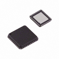
AD5412ACPZ-REEL7 Analog Devices Inc, AD5412ACPZ-REEL7 Datasheet - Page 31

AD5412ACPZ-REEL7
Manufacturer Part Number
AD5412ACPZ-REEL7
Description
12Bit 1V, I Out DAC
Manufacturer
Analog Devices Inc
Datasheet
1.AD5412ACPZ-REEL7.pdf
(40 pages)
Specifications of AD5412ACPZ-REEL7
Design Resources
Simplified 12-Bit Voltage and 4 mA-to-20 mA Output Solution Using AD5412 (CN0097)
Settling Time
25µs
Number Of Bits
12
Data Interface
MICROWIRE™, Serial, SPI™
Number Of Converters
1
Voltage Supply Source
Analog and Digital, Dual ±
Power Dissipation (max)
128mW
Operating Temperature
-40°C ~ 85°C
Mounting Type
Surface Mount
Package / Case
40-LFCSP
Number Of Channels
1
Resolution
12b
Conversion Rate
40KSPS
Interface Type
SER 3W SPI QSPI UW
Single Supply Voltage (typ)
12/15/18/24/28V
Architecture
R-2R
Power Supply Requirement
Single/Dual
Output Type
Current/Voltage
Single Supply Voltage (min)
10.8V
Single Supply Voltage (max)
40V
Dual Supply Voltage (min)
0/10.8V
Dual Supply Voltage (max)
-26.4/40V
Operating Temp Range
-40C to 85C
Operating Temperature Classification
Industrial
Mounting
Surface Mount
Pin Count
40
Lead Free Status / RoHS Status
Lead free / RoHS Compliant
Lead Free Status / RoHS Status
Lead free / RoHS Compliant
Other names
AD5412ACPZ-REEL7TR
Available stocks
Company
Part Number
Manufacturer
Quantity
Price
Company:
Part Number:
AD5412ACPZ-REEL7
Manufacturer:
Aptina
Quantity:
1 500
AD5412/AD5422 FEATURES
FAULT ALERT
The AD5412/AD5422 are equipped with a FAULT pin, which
is an open-drain output allowing several AD5412/AD5422
devices to be connected together to one pull-up resistor for
global fault detection. The FAULT pin is forced active by one
of the following fault scenarios:
•
•
The I
in conjunction with the FAULT pin to inform the user which
one of the fault conditions caused the FAULT pin to be asserted
(see
VOLTAGE OUTPUT SHORT CIRCUIT PROTECTION
Under normal operation, the voltage output sinks/sources
10 mA. The maximum current that the voltage output delivers
is ~20 mA; this is the short-circuit current.
VOLTAGE OUTPUT OVERRANGE
An overrange facility is provided on the voltage output. When
enabled via the control register, the selected output range is
overranged by, typically, 10%.
VOLTAGE OUTPUT FORCE-SENSE
The +V
sensing of the load connected to the voltage output. If the load
is connected at the end of a long or high impedance cable,
sensing the voltage at the load allows the output amplifier to
compensate and ensure that the correct voltage is applied across
the load. This function is limited only by the available power
supply headroom.
Table 19
The voltage at I
range, due to an open-loop circuit or insufficient power
supply voltage. The I
transistor and internal amplifier, as shown in Figure 64.
The internal circuitry that develops the fault output avoids
using a comparator with window limits because this would
require an actual output error before the FAULT output
becomes active. Instead, the signal is generated when the
internal amplifier in the output stage has less than ~1 V
of remaining drive capability (when the gate of the output
PMOS transistor nearly reaches ground). Thus, the FAULT
output activates slightly before the compliance limit is
reached. Because the comparison is made within the
feedback loop of the output amplifier, the output accuracy
is maintained by its open-loop gain, and an output error
does not occur before the FAULT output becomes active.
If the core temperature of the AD5412/AD5422 exceeds
approximately 150°C.
OUT
SENSE
fault and over temp bits of the status register are used
and −V
and
Table 20
SENSE
OUT
attempts to rise above the compliance
pins are provided to facilitate remote
OUT
).
current is controlled by a PMOS
Rev. C | Page 31 of 40
ASYNCHRONOUS CLEAR (CLEAR)
The CLEAR pin is an active high clear that allows the voltage
output to be cleared to either zero-scale code or midscale code,
user selectable via the CLEAR SELECT pin, or the CLRSEL bit
of the control register, as described in Table 21. (The clear select
feature is a logical OR function of the CLEAR SELECT pin and
the CLRSEL bit.) The current output clears to the bottom of its
programmed range. It is necessary for CLEAR to be high for a
minimum amount of time to complete the operation (see
Figure 2). When the CLEAR signal is returned low, the output
remains at the cleared value. The preclear value can be restored
by pulsing the LATCH signal low without clocking any data. A
new value cannot be programmed until the CLEAR pin is
returned low.
Table 21. CLRSEL Options
CLRSEL
0
1
In addition to defining the output value for a clear operation,
the CLRSEL bit and CLEAR SELECT pin also define the default
output value. During selection of a new voltage range, the
output value is as defined in Table 21. To avoid glitches on the
output, it is recommended that, before changing voltage ranges,
the user disable the output by setting the OUTEN bit of the
control register to logic low. When OUTEN is set to logic high,
the output goes to the default value as defined by CLRSEL and
CLEAR SELECT.
INTERNAL REFERENCE
The AD5412/AD5422 contain an integrated 5 V voltage
reference with initial accuracy of ±5 mV maximum and a
temperature drift coefficient of ±10 ppm/°C maximum. The
reference voltage is buffered and externally available for use
elsewhere within the system. See Figure 16 for a load regulation
graph of the integrated reference.
EXTERNAL CURRENT SETTING RESISTOR
R
conversion circuitry (see Figure 64). The stability of the output
current over temperature is dependent on the stability of the
value of R
output current over temperature, an external precision 15 kΩ
low drift resistor can be connected to the R
AD5412/AD5422 to be used instead of the internal resistor
(R
(see Table 14).
SET
SET
is an internal sense resistor as part of the voltage-to-current
). The external resistor is selected via the control register
SET
Unipolar Output Range
0 V
Midscale
. As a method of improving the stability of the
Output Value
AD5412/AD5422
Bipolar Output Range
0 V
Negative full scale
SET
pin of the


