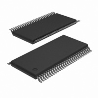
74ALVCH16821DGG:11 NXP Semiconductors, 74ALVCH16821DGG:11 Datasheet - Page 8

74ALVCH16821DGG:11
Manufacturer Part Number
74ALVCH16821DGG:11
Description
74ALVCH16821DGG/TSSOP56/TUBE-B
Manufacturer
NXP Semiconductors
Series
74ALVCHr
Type
D-Type Busr
Datasheet
1.74ALVCH16821DGG11.pdf
(12 pages)
Specifications of 74ALVCH16821DGG:11
Function
Standard
Output Type
Tri-State Non Inverted
Number Of Elements
2
Number Of Bits Per Element
10
Frequency - Clock
250MHz
Delay Time - Propagation
2.6ns
Trigger Type
Positive Edge
Current - Output High, Low
24mA, 24mA
Voltage - Supply
2.3 V ~ 2.7 V
Operating Temperature
-40°C ~ 85°C
Mounting Type
Surface Mount
Package / Case
56-TSSOP
Lead Free Status / RoHS Status
Lead free / RoHS Compliant
Other names
74ALVCH16821DG
74ALVCH16821DG
935259010112
74ALVCH16821DG
935259010112
1. V
2. V
3. V
4. V
5. V
1. V
2. V
3. V
4. V
5. V
Philips Semiconductors
AC WAVEFORMS
V
V
1998 May 29
CC
CC
Waveform 1.
20-bit bus-interface D-type flip-flop;
positive-edge trigger (3-State)
nQ
OUTPUT
LOW-to-OFF
OFF-to-LOW
OUTPUT
HIGH-to-OFF
OFF-to-HIGH
the output load.
the output load.
nOE INPUT
nCP INPUT
= 2.3 TO 2.7 V RANGE
= 3.0 TO 3.6 V RANGE AND V
M
X
Y
I
OL
M
X
Y
I
OL
n
GND
V
V
V
GND
= V
= 2.7 V
V
OL
OH
OUTPUT
CC
Waveform 2. The 3-State enable and disable times.
= V
= V
= V
= V
= 0.5 V
= 1.5 V
I
and V
and V
CC
GND
V
OL
OH
OL
OH
V
OH
OL
V
I
+ 0.15V
+ 0.3V
– 0.15V
– 0.3V
OH
OH
are the typical output voltage drop that occur with
are the typical output voltage drop that occur with
The input (nCP) to output propagation delays.
outputs
enabled
V
V
M
t
M
PHL
t
PLZ
t
t
PHZ
w
1/f
MAX
V
M
V
X
V
Y
CC
= 2.7 V
outputs
disabled
t
PLH
t
PZL
t
PZH
V
V
M
M
V
SH00128
M
SW00308
outputs
enabled
8
TEST CIRCUIT
GENERATOR
t
t
PLZ/
PHZ/
PULSE
SWITCH POSITION
t
PLH/
TEST
DEFINITIONS
nQ
R
C
R
Waveform 4. Load circuitry for switching times
t
t
L
L
T
PZL
PZH
nCP INPUT
nD
t
n
= Load resistor
= Load capacitance includes jig and probe capacitance
= Termination resistance should be equal to Z
PHL
OUTPUT
n
INPUT
Waveform 3. Set up and hold times.
GND
GND
V
V
OH
OL
V
V
Test Circuit for switching times
I
I
2 < V
Open
V
GND
I
S
1
R
T
CC
V
M
t
V
su
D.U.T.
V
M
CC
2.7–3.6V
t
< 2.7V
h
74ALVCH16821
V
CC
V
V
O
M
C
L
OUT
2.7V
V
V
Product specification
CC
I
of pulse generators.
t
su
SH00129
t
h
S
1
R
R
SV00906
L
L
= 500
= 500
2 * V
Open
GND
CC


