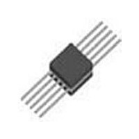
5962-9553601QXA National Semiconductor, 5962-9553601QXA Datasheet - Page 19

5962-9553601QXA
Manufacturer Part Number
5962-9553601QXA
Description
VERY HI SPD, HI CURRENT OP AMP
Manufacturer
National Semiconductor
Type
Voltage Feedback Amplifierr
Datasheet
1.5962-9553601QXA.pdf
(24 pages)
Specifications of 5962-9553601QXA
Rail/rail I/o Type
No
Number Of Elements
1
Unity Gain Bandwidth Product
170MHz
Slew Rate
2000V/us
Common Mode Rejection Ratio
80dB
Input Offset Voltage
1.5mV
Input Bias Current
10uA
Single Supply Voltage (typ)
9/12/15/18/24/28V
Dual Supply Voltage (typ)
±3/±5/±9/±12/±15V
Power Dissipation
730mW
Voltage Gain In Db
75dB
Power Supply Rejection Ratio
85dB
Power Supply Requirement
Single/Dual
Shut Down Feature
No
Single Supply Voltage (min)
5.5V
Single Supply Voltage (max)
36V
Dual Supply Voltage (min)
±2.75V
Dual Supply Voltage (max)
±18V
Technology
BiCOM
Operating Temp Range
-55C to 125C
Operating Temperature Classification
Military
Mounting
Surface Mount
Pin Count
10
Package Type
CPAK
Number Of Channels
1
Voltage Gain Db
75 dB
Common Mode Rejection Ratio (min)
80 dB
Operating Supply Voltage
9 V, 12 V, 15 V, 18 V, 24 V, 28 V
Supply Current
8 mA at +/- 5 V
Maximum Power Dissipation
730 mW
Maximum Operating Temperature
+ 125 C
Package / Case
CPAK
Maximum Dual Supply Voltage
+/- 18 V
Minimum Operating Temperature
- 55 C
Lead Free Status / Rohs Status
Not Compliant
Power Dissipation
The maximum power allowed to dissipate in a device is de-
fined as:
Where
θ
For example, for the LM7171 in a Ceramic SOIC package, the
maximum power dissipation at 25°C ambient temperature is
680 mW.
Thermal resistance, θ
size, package size and package material. The smaller the die
size and package, the higher θ
package has a lower thermal resistance (106°C/W) than that
of the Ceramic SOIC (182°C/W). Therefore, for higher dissi-
pation capability, use an 8-pin DIP package.
The total power dissipated in a device can be calculated as:
P
connected at the output. P
vice with a load connected at the output; it is not the power
dissipated by the load.
Furthermore,
For example, the total power dissipated by the LM7171 with
V
Q
S
PD
T
T
P
P
P
= ±15V and output voltage of 10V into 1 kΩ is
is the quiescent power dissipated in a device with no load
JA
J(max)
A
Q
L
D
: = output current × (voltage difference between sup-
: = supply current × total supply voltage with no load
FIGURE 6. The LM7171 Driving a 150 pF Load
= P
is the power dissipation in a device
is the maximum junction temperature
is the ambient temperature
is the thermal resistance of a particular package
ply voltage and output voltage of the same side of
supply voltage)
Q
+ P
with a 50Ω Isolation Resistor
L
P
D
JA
= (T
, depends on parameters such as die
P
D
L
J(max)
= P
is the power dissipated in the de-
Q
− T
JA
+ P
becomes. The 8-pin DIP
A
L
)/θ
JA
20159513
19
Application Circuit
= (6.5 mA) × (30V) + (10 mA) × (15V − 10V)
= 195 mW + 50 mW
= 245 mW
Fast Instrumentation Amplifier
Multivibrator
20159581
20159580
www.national.com
20159515
20159514


