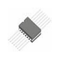
5962-8773901XA National Semiconductor, 5962-8773901XA Datasheet

5962-8773901XA
Specifications of 5962-8773901XA
Related parts for 5962-8773901XA
5962-8773901XA Summary of contents
Page 1
... WG14A E20A J14A 5962R9673801VCA J14A 100 krad(Si) 5962R9673802VCA J14A 100 krad(Si) 5962–9673801VDA W14B W14B 5962–9673801VXA WG14A WG14A 5962R9673801VXA WG14A 100 krad(Si) 5962R9673802VXA WG14A 100 krad(Si) 5962R9673801VDA W14B 100 krad(Si) 201221 October 15, 2010 100 krad(Si) 100 krad(Si ±1 to ± ...
Page 2
... Connection Diagrams www.national.com SMD Part Number NS Package Number Package Description 5962R9673802VDA W14B 100 krad(Si) 5962R9673802V9A (Note 1) 100 krad(Si) 5962R9673801V9A (Note 1) 100 krad(Si) Dual-In-Line Package See NS Package NumberJ14A See NS Package Number W14B, WG14A See NS Package Number E20A 2 14LD CERPACK Bare Die Bare Die ...
Page 3
Absolute Maximum Ratings Supply Voltage Differential Input Voltage (Note 8) Input Voltage Input Current (V < −0 (Note IN DC Power Dissipation (Note 5, Note 14) LCC CERDIP CERPACK SOIC Sink Current (approx) (Note 12) Output ...
Page 4
Quality Conformance Inspection Mil-Std-883, Method 5005 — Group A Subgroup www.national.com Description Static tests at Static tests at Static tests at Dynamic tests at Dynamic tests at Dynamic ...
Page 5
LM139 883 Electrical Characteristics DC Parameters The following conditions apply, unless otherwise specified 5V, V Symbol Parameters I Supply Current CC Supply Current V Input Offset Voltage IO CMRR Common Mode Rejection Ratio PSRR Power Supply Rejection Ratio ...
Page 6
... LM139A SMD 5962–8773901 Electrical Characteristics DC Parameters The following conditions apply, unless otherwise specified 5V, V Symbol Parameter I Supply Current CC I Output Leakage Current CEX V Saturation Voltage Sat I Output Sink Current Sink V Input Offset Voltage IO ±I Input Bias Current IB I Input Offset Current ...
Page 7
... LM139A 883, QMLV & RH, SMD 5962–9673801 Electrical Characteristics DC Parameters (Note 11, The following conditions apply, unless otherwise specified 5V, V Symbol Parameters I Supply Current CC I Output Leakage Current CEX V Saturation Voltage Sat I Output Sink Current Sink V Input Offset Voltage IO ± I Input Bias Current ...
Page 8
DC Parameters Delta Values The following conditions apply, unless otherwise specified 5V, V Deltas required for S-Level, MLS (as specified on Internal Processing instructions (IPI)), and QMLV product at Group B, Subgroup 5. Symbol Parameters V Input Offset ...
Page 9
... These parts may be dose rate sensitive in a space environment and demonstrate enhanced low dose rate effect. Radiation end point limits for the noted parameters are guaranteed only for the conditions as specified in Mil-Std-883, Method 1019, Condition A. Note 12: SMD 5962–8773901 only Note 13: Human Body model, 1.5 KΩ in series with 100 pF ...
Page 10
Typical Performance Characteristics Supply Current Output Saturation Voltage Response Time for Various Input Overdrives —Positive Transition www.national.com LM139, LM139A 20122134 Response Time for Various Input Overdrives —Negative Transition 20122136 20122138 10 Input Current 20122135 20122137 ...
Page 11
Application Hints The LM139 series are high gain, wide bandwidth devices which, like most comparators, can easily oscillate if the output lead is inadvertently allowed to capacitively couple to the in- puts via stray capacitance. This shows up only during ...
Page 12
Typical Applications ( www.national.com One-Shot Multivibrator Bi-Stable Multivibrator 12 20122110 20122111 ...
Page 13
One-Shot Multivibrator with Input Lock Out Pulse Generator 13 20122112 20122117 www.national.com ...
Page 14
Large Fan-In AND Gate www.national.com ORing the Outputs 20122113 14 20122115 ...
Page 15
Non-Inverting Comparator with Hysteresis Time Delay Generator Inverting Comparator with Hysteresis 20122118 15 20122114 20122119 www.national.com ...
Page 16
Squarewave Oscillator Limit Comparator www.national.com Basic Comparator 20122116 Comparing Input Voltages of Opposite Polarity 20122124 16 20122121 20122120 ...
Page 17
Output Strobing * Or open-collector logic gate without pull-up resistor Crystal Controlled Oscillator 20122122 17 20122125 www.national.com ...
Page 18
www.national.com 18 ...
Page 19
Transducer Amplifier Split-Supply Applications ( +15 V and V − = − Zero Crossing Detector (Single Power Supply) 20122128 MOS Clock Driver 19 20122130 20122131 www.national.com ...
Page 20
Zero Crossing Detector Schematic Diagram www.national.com Comparator With a Negative Reference 20122132 20 20122133 20122101 ...
Page 21
... B Features, Ordering Information Table, Rad Hard Electrical Section and Notes 02/13/08 C Features, Ordering Table, LM139A 883, QMLV & RH, SMD 5962–9673801 Electrical Characteristics, Notes 10/15/2010 D Data Sheet Title, Ordering Table, Changes 3 MDS datasheets converted into one Corp. datasheet format. MNLM139A-X-RH rev 4B0, MDLM139A-X rev 0C1, MNLM139– ...
Page 22
Physical Dimensions www.national.com inches (millimeters) unless otherwise noted Leadless Chip Carrier (E)) NS Package Number E20A Ceramic Dual-In-Line Package (J) NS Package Number J14A 22 ...
Page 23
Ceramic Flat Package (W) NS Package Number W14B Ceramic SOIC (WG) NS Package Number WG14A 23 www.national.com ...
Page 24
... For more National Semiconductor product information and proven design tools, visit the following Web sites at: www.national.com Products Amplifiers www.national.com/amplifiers Audio www.national.com/audio Clock and Timing www.national.com/timing Data Converters www.national.com/adc Interface www.national.com/interface LVDS www.national.com/lvds Power Management www.national.com/power Switching Regulators www.national.com/switchers LDOs www.national.com/ldo LED Lighting www ...


