MJD112 ON Semiconductor, MJD112 Datasheet - Page 7
MJD112
Manufacturer Part Number
MJD112
Description
Darlington Transistors 2A 100V Bipolar
Manufacturer
ON Semiconductor
Datasheet
1.MJD112.pdf
(8 pages)
Specifications of MJD112
Configuration
Single
Transistor Polarity
NPN
Mounting Style
SMD/SMT
Package / Case
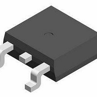
TO-252-3 (DPAK)
Collector- Emitter Voltage Vceo Max
100 V
Emitter- Base Voltage Vebo
5 V
Collector- Base Voltage Vcbo
100 V
Maximum Dc Collector Current
2 A
Maximum Collector Cut-off Current
20 uA
Power Dissipation
20 W
Maximum Operating Temperature
+ 150 C
Continuous Collector Current
2 A
Dc Collector/base Gain Hfe Min
200, 500, 1000
Minimum Operating Temperature
- 65 C
Lead Free Status / RoHS Status
Lead free / RoHS Compliant
Available stocks
Company
Part Number
Manufacturer
Quantity
Price

Company:
Part Number:
MJD112-1G
Manufacturer:
ON Semiconductor
Quantity:
1 900
Company:
Part Number:
MJD112-1G
Manufacturer:
ON
Quantity:
12 500
Company:
Part Number:
MJD112-RTF/P
Manufacturer:
KEC
Quantity:
550
Part Number:
MJD112-TP
Manufacturer:
MCC/美微科
Quantity:
20 000
Company:
Part Number:
MJD112G
Manufacturer:
ON
Quantity:
12 500
Part Number:
MJD112RL
Manufacturer:
MOTOROLA/摩托罗拉
Quantity:
20 000
Part Number:
MJD112T4
Manufacturer:
ST
Quantity:
20 000


L3
L4
b2
e
1
b3
4
2
E
3
b
A
D
0.005 (0.13)
B
*For additional information on our Pb−Free strategy and soldering
details, please download the ON Semiconductor Soldering and
Mounting Techniques Reference Manual, SOLDERRM/D.
M
DETAIL A
0.228
C
5.80
c
L2
A
GAUGE
PLANE
PACKAGE DIMENSIONS
SOLDERING FOOTPRINT*
ROTATED 90 CW
0.244
0.101
6.20
c2
2.58
DETAIL A
H
C
http://onsemi.com
L
CASE 369C−01
L1
ISSUE D
DPAK
5
7
A1
0.118
3.0
H
0.063
1.6
SCALE 3:1
C
Z
SEATING
PLANE
6.172
0.243
inches
NOTES:
mm
1. DIMENSIONING AND TOLERANCING PER ASME
2. CONTROLLING DIMENSION: INCHES.
3. THERMAL PAD CONTOUR OPTIONAL WITHIN DI-
4. DIMENSIONS D AND E DO NOT INCLUDE MOLD
5. DIMENSIONS D AND E ARE DETERMINED AT THE
6. DATUMS A AND B ARE DETERMINED AT DATUM
Y14.5M, 1994.
MENSIONS b3, L3 and Z.
FLASH, PROTRUSIONS, OR BURRS. MOLD
FLASH, PROTRUSIONS, OR GATE BURRS SHALL
NOT EXCEED 0.006 INCHES PER SIDE.
OUTERMOST EXTREMES OF THE PLASTIC BODY.
PLANE H.
STYLE 1:
DIM
A1
b2
b3
c2
L1
L2
L3
L4
PIN 1. BASE
A
b
D
E
H
L
Z
c
e
2. COLLECTOR
3. EMITTER
4. COLLECTOR
0.086
0.000
0.025
0.030
0.180
0.018
0.018
0.235
0.250
0.370
0.055
0.035
0.155
MIN
−−−
0.090 BSC
0.108 REF
0.020 BSC
INCHES
0.094
0.005
0.035
0.045
0.215
0.024
0.024
0.245
0.265
0.410
0.070
0.050
0.040
MAX
−−−
MILLIMETERS
2.18
0.00
0.63
0.76
4.57
0.46
0.46
5.97
6.35
9.40
1.40
0.89
3.93
MIN
−−−
2.29 BSC
2.74 REF
0.51 BSC
10.41
MAX
2.38
0.13
0.89
1.14
5.46
0.61
0.61
6.22
6.73
1.78
1.27
1.01
−−−
Related parts for MJD112
Image
Part Number
Description
Manufacturer
Datasheet
Request
R

Part Number:
Description:
ON Semiconductor [VOLTAGE REGULATOR]
Manufacturer:
ON Semiconductor
Datasheet:
Part Number:
Description:
357-036-542-201 CARDEDGE 36POS DL .156 BLK LOPRO
Manufacturer:
ON Semiconductor
Datasheet:
Part Number:
Description:
357-036-542-201 CARDEDGE 36POS DL .156 BLK LOPRO
Manufacturer:
ON Semiconductor
Datasheet:
Part Number:
Description:
357-036-542-201 CARDEDGE 36POS DL .156 BLK LOPRO
Manufacturer:
ON Semiconductor
Datasheet:
Part Number:
Description:
357-036-542-201 CARDEDGE 36POS DL .156 BLK LOPRO
Manufacturer:
ON Semiconductor
Datasheet:
Part Number:
Description:
357-036-542-201 CARDEDGE 36POS DL .156 BLK LOPRO
Manufacturer:
ON Semiconductor
Datasheet:
Part Number:
Description:
357-036-542-201 CARDEDGE 36POS DL .156 BLK LOPRO
Manufacturer:
ON Semiconductor
Datasheet:
Part Number:
Description:
357-036-542-201 CARDEDGE 36POS DL .156 BLK LOPRO
Manufacturer:
ON Semiconductor
Datasheet:
Part Number:
Description:
357-036-542-201 CARDEDGE 36POS DL .156 BLK LOPRO
Manufacturer:
ON Semiconductor
Datasheet:
Part Number:
Description:
357-036-542-201 CARDEDGE 36POS DL .156 BLK LOPRO
Manufacturer:
ON Semiconductor
Datasheet:
Part Number:
Description:
357-036-542-201 CARDEDGE 36POS DL .156 BLK LOPRO
Manufacturer:
ON Semiconductor
Datasheet:
Part Number:
Description:
Manufacturer:
ON Semiconductor
Datasheet:
Part Number:
Description:
Manufacturer:
ON Semiconductor
Datasheet:
Part Number:
Description:
Manufacturer:
ON Semiconductor
Datasheet: