MJD112 ON Semiconductor, MJD112 Datasheet

Darlington Transistors 2A 100V Bipolar

MJD112

Manufacturer Part Number
MJD112
Description
Darlington Transistors 2A 100V Bipolar
Manufacturer
ON Semiconductor
Datasheet

Specifications of MJD112

Configuration
Single
Transistor Polarity
NPN
Mounting Style
SMD/SMT
Package / Case
TO-252-3 (DPAK)
Collector- Emitter Voltage Vceo Max
100 V
Emitter- Base Voltage Vebo
5 V
Collector- Base Voltage Vcbo
100 V
Maximum Dc Collector Current
2 A
Maximum Collector Cut-off Current
20 uA
Power Dissipation
20 W
Maximum Operating Temperature
+ 150 C
Continuous Collector Current
2 A
Dc Collector/base Gain Hfe Min
200, 500, 1000
Minimum Operating Temperature
- 65 C
Lead Free Status / RoHS Status
Lead free / RoHS Compliant

Available stocks

Company
Part Number
Manufacturer
Quantity
Price
Part Number:
MJD112
Manufacturer:
ON
Quantity:
100
Part Number:
MJD112
Manufacturer:
ST
0
Part Number:
MJD112 @@@@@@@@@@
Manufacturer:
ST
0
Part Number:
MJD112 @@@@@@@@@@
Manufacturer:
ST
0
Part Number:
MJD112--252
Manufacturer:
ST
0
Part Number:
MJD112-03
Manufacturer:
ST
0
Part Number:
MJD112-1G
Manufacturer:
ON Semiconductor
Quantity:
1 900
Part Number:
MJD112-1G
Manufacturer:
ON
Quantity:
12 500
Part Number:
MJD112-RTF/P
Manufacturer:
KEC
Quantity:
550
Part Number:
MJD112-TP
Manufacturer:
MCC/美微科
Quantity:
20 000
Part Number:
MJD112G
Manufacturer:
ON
Quantity:
12 500
Part Number:
MJD112RL
Manufacturer:
MOTOROLA/摩托罗拉
Quantity:
20 000
Part Number:
MJD112T4
Manufacturer:
ST
Quantity:
20 000
MJD112 (NPN)
MJD117 (PNP)
Complementary Darlington
Power Transistors
DPAK For Surface Mount Applications
driver stages in applications such as switching regulators, converters,
and power amplifiers.
Features
Stresses exceeding Maximum Ratings may damage the device. Maximum
Ratings are stress ratings only. Functional operation above the Recommended
Operating Conditions is not implied. Extended exposure to stresses above the
Recommended Operating Conditions may affect device reliability.
1. These ratings are applicable when surface mounted on the minimum pad
© Semiconductor Components Industries, LLC, 2011
March, 2011 − Rev. 9
MAXIMUM RATINGS
THERMAL CHARACTERISTICS
Collector−Emitter Voltage
Collector−Base Voltage
Emitter−Base Voltage
Collector Current
Base Current
Total Power Dissipation @ T
Total Power Dissipation (Note1)
Operating and Storage Junction
Thermal Resistance, Junction−to−Case
Thermal Resistance, Junction−to−Ambient
(Note 1)
Designed for general purpose power and switching such as output or
(No Suffix)
Lead Formed for Surface Mount Applications in Plastic Sleeves
Straight Lead Version in Plastic Sleeves (“−1” Suffix)
Electrically Similar to Popular TIP31 and TIP32 Series
Pb−Free Packages are Available
sizes recommended.
Derate above 25°C
@ T
Derate above 25°C
Temperature Range
A
= 25°C
Characteristic
Rating
− Continuous
− Peak
C
= 25°C
Symbol
Symbol
T
V
R
R
J
V
V
P
P
, T
CEO
I
I
qJC
qJA
CB
EB
C
B
D
D
stg
−65 to +150
0.014
Max
0.16
1.75
Max
6.25
71.4
100
100
50
20
5
2
4
1
mAdc
W/°C
W/°C
°C/W
°C/W
Unit
Unit
Vdc
Vdc
Vdc
Adc
°C
W
W
1 2
See detailed ordering and shipping information in the package
dimensions section on page 6 of this data sheet.
1
2
3
3
POWER TRANSISTORS
100 VOLTS, 20 WATTS
ORDERING INFORMATION
4
4
CASE 369D
A
Y
WW
x
G
DPAK−3
http://onsemi.com
2 AMPERES
CASE 369C
SILICON
DPAK
= Assembly Location
= Year
= Work Week
= 2 or 7
= Pb−Free Package
Publication Order Number:
DIAGRAMS
MARKING
AYWW
J11xG
J11xG
YWW
MJD112/D

Related parts for MJD112

MJD112 Summary of contents

Page 1

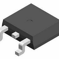
... MJD112 (NPN) MJD117 (PNP) Complementary Darlington Power Transistors DPAK For Surface Mount Applications Designed for general purpose power and switching such as output or driver stages in applications such as switching regulators, converters, and power amplifiers. Features • Lead Formed for Surface Mount Applications in Plastic Sleeves (No Suffix) • ...

Page 2

... APPROX 25 ms -12 V FOR t AND t ≤ AND DUTY CYCLE = 1% FOR NPN TEST CIRCUIT REVERSE ALL POLARITIES. Figure 1. Switching Times Test Circuit (T = 25_C unless otherwise noted) C MJD117 MJD112 SCOPE TUT B 1 0.8 ≈ ≈ 0 0 DISCONNECTED r 1 0.2 0.04 http://onsemi.com 2 Î Î Î Î Î ...

Page 3

D = 0.5 0.5 0.3 0.2 0.2 0.1 0.05 0.1 0.07 0.01 0.05 0.03 SINGLE PULSE 0.02 0.01 0.01 0.02 0.03 0.05 0 0.7 0.5 dc 0.3 0.2 ...

Page 4

... TYPICAL ELECTRICAL CHARACTERISTICS NPN MJD112 125° 25° 800 - 55°C 600 400 300 0.04 0.06 0.1 0.2 0.4 0 COLLECTOR CURRENT (AMP 0 2.2 1.8 1.4 1 0.6 0.1 0.2 0 BASE CURRENT (mA 25° 250 BE(sat 1 250 CE(sat 0.6 ...

Page 5

... NPN MJD112 + 0.8 *APPLIED FOR I /I < 0.8 25°C TO 150°C - 1.6 *q FOR V - 2.4 VC CE(sat) - 55°C TO 25°C - 3.2 25°C TO 150°C q FOR 55°C TO 25°C - 4.8 0.04 0.06 0.1 0.2 0.4 0 COLLECTOR CURRENT (AMP REVERSE FORWARD 150° 100°C 25°C ...

Page 6

... ORDERING INFORMATION Device MJD112 MJD112G MJD112−001 MJD112−1G MJD112RL MJD112RLG MJD112T4 MJD112T4G MJD117 MJD117G MJD117−001 MJD117−1G MJD117T4 MJD117T4G †For information on tape and reel specifications, including part orientation and tape sizes, please refer to our Tape and Reel Packaging Specifications Brochure, BRD8011/D. ...

Page 7

... DETAIL 0.005 (0.13 5.80 0.228 *For additional information on our Pb−Free strategy and soldering details, please download the ON Semiconductor Soldering and Mounting Techniques Reference Manual, SOLDERRM/D. PACKAGE DIMENSIONS DPAK CASE 369C−01 ISSUE GAUGE SEATING L2 C PLANE PLANE DETAIL A ROTATED SOLDERING FOOTPRINT* 6 ...

Page 8

... R 0.180 0.215 4.45 5.45 S 0.025 0.040 0.63 1.01 V 0.035 0.050 0.89 1.27 Z 0.155 −−− 3.93 −−− ON Semiconductor Website: www.onsemi.com Order Literature: http://www.onsemi.com/orderlit For additional information, please contact your local Sales Representative MJD112/D ...

Related keywords