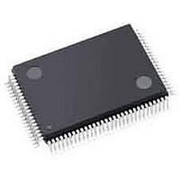
C8051F124TB Silicon Laboratories Inc, C8051F124TB Datasheet - Page 205

C8051F124TB
Manufacturer Part Number
C8051F124TB
Description
MCU, MPU & DSP Development Tools With C8051F124 MCU
Manufacturer
Silicon Laboratories Inc
Datasheet
1.C8051F120DK.pdf
(350 pages)
Specifications of C8051F124TB
Processor To Be Evaluated
C8051F12x and C8051F13x
Interface Type
USB
Lead Free Status / RoHS Status
Lead free / RoHS Compliant
- Current page: 205 of 350
- Download datasheet (2Mb)
Flash Read Lock Byte
Bits7–0: Each bit locks a corresponding block of memory. (Bit7 is MSB).
Flash Write/Erase Lock Byte
Bits7–0: Each bit locks a corresponding block of memory.
Flash access Limit Register (FLACL)
Read and Write/Erase Security Bits.
(Bit 7 is MSB.)
Bit
7
6
5
4
3
2
1
0
0x0C000 - 0x0FFFF
0x08000 - 0x0BFFF
0x04000 - 0x07FFF
0x00000 - 0x03FFF
Memory Block
0: Read operations are locked (disabled) for corresponding block across the JTAG interface.
1: Read operations are unlocked (enabled) for corresponding block across the JTAG inter-
face.
0: Write/Erase operations are locked (disabled) for corresponding block across the JTAG
interface.
1: Write/Erase operations are unlocked (enabled) for corresponding block across the JTAG
interface.
NOTE: When the highest block is locked, the security bytes may be written but not erased.
The Flash Access Limit is defined by the setting of the FLACL register, as described in SFR
Definition 15.1. Firmware running at or above this address is prohibited from using the
MOVX and MOVC instructions to read, write, or erase Flash locations below this address.
Figure 15.3. 64 kB Flash Memory Map and Security Bytes
N/A
N/A
N/A
N/A
Write/Erase Lock Byte
Read Lock Byte
Memory Space
Program/Data
SFLE = 0
Rev. 1.4
C8051F120/1/2/3/4/5/6/7
0x0FFFF
0x0FFFE
0x0FFFD
0x00000
Flash Access Limit
C8051F130/1/2/3
Scratchpad Memory
SFLE = 1
(Data only)
0x00FF
0x0000
205
Related parts for C8051F124TB
Image
Part Number
Description
Manufacturer
Datasheet
Request
R
Part Number:
Description:
SMD/C°/SINGLE-ENDED OUTPUT SILICON OSCILLATOR
Manufacturer:
Silicon Laboratories Inc
Part Number:
Description:
Manufacturer:
Silicon Laboratories Inc
Datasheet:
Part Number:
Description:
N/A N/A/SI4010 AES KEYFOB DEMO WITH LCD RX
Manufacturer:
Silicon Laboratories Inc
Datasheet:
Part Number:
Description:
N/A N/A/SI4010 SIMPLIFIED KEY FOB DEMO WITH LED RX
Manufacturer:
Silicon Laboratories Inc
Datasheet:
Part Number:
Description:
N/A/-40 TO 85 OC/EZLINK MODULE; F930/4432 HIGH BAND (REV E/B1)
Manufacturer:
Silicon Laboratories Inc
Part Number:
Description:
EZLink Module; F930/4432 Low Band (rev e/B1)
Manufacturer:
Silicon Laboratories Inc
Part Number:
Description:
I°/4460 10 DBM RADIO TEST CARD 434 MHZ
Manufacturer:
Silicon Laboratories Inc
Part Number:
Description:
I°/4461 14 DBM RADIO TEST CARD 868 MHZ
Manufacturer:
Silicon Laboratories Inc
Part Number:
Description:
I°/4463 20 DBM RFSWITCH RADIO TEST CARD 460 MHZ
Manufacturer:
Silicon Laboratories Inc
Part Number:
Description:
I°/4463 20 DBM RADIO TEST CARD 868 MHZ
Manufacturer:
Silicon Laboratories Inc
Part Number:
Description:
I°/4463 27 DBM RADIO TEST CARD 868 MHZ
Manufacturer:
Silicon Laboratories Inc
Part Number:
Description:
I°/4463 SKYWORKS 30 DBM RADIO TEST CARD 915 MHZ
Manufacturer:
Silicon Laboratories Inc
Part Number:
Description:
N/A N/A/-40 TO 85 OC/4463 RFMD 30 DBM RADIO TEST CARD 915 MHZ
Manufacturer:
Silicon Laboratories Inc
Part Number:
Description:
I°/4463 20 DBM RADIO TEST CARD 169 MHZ
Manufacturer:
Silicon Laboratories Inc


