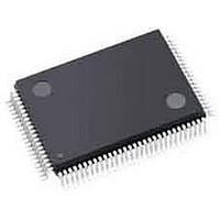
C8051F124TB Silicon Laboratories Inc, C8051F124TB Datasheet - Page 117

C8051F124TB
Manufacturer Part Number
C8051F124TB
Description
MCU, MPU & DSP Development Tools With C8051F124 MCU
Manufacturer
Silicon Laboratories Inc
Datasheet
1.C8051F120DK.pdf
(350 pages)
Specifications of C8051F124TB
Processor To Be Evaluated
C8051F12x and C8051F13x
Interface Type
USB
Lead Free Status / RoHS Status
Lead free / RoHS Compliant
- Current page: 117 of 350
- Download datasheet (2Mb)
9.3.
On the C8051F130/1/2/3 devices, the VREF0 pin provides a voltage reference input for ADC0, which can
be connected to an external precision reference or the internal voltage reference, as shown in Figure 9.3.
The REF0CN register for the C8051F130/1/2/3 is described in SFR Definition 9.3.
Bits7–5: UNUSED. Read = 000b; Write = don’t care.
Bits4–3: Reserved: Must be written to 0.
Bit2:
Bit1:
Bit0:
SFR Page:
SFR Address:
Figure 9.3. Voltage Reference Functional Block Diagram (C8051F130/1/2/3)
R/W
Bit7
-
Reference Configuration on the C8051F130/1/2/3
SFR Definition 9.3. REF0CN: Reference Control (C8051F130/1/2/3)
TEMPE: Temperature Sensor Enable Bit.
0: Internal Temperature Sensor Off.
1: Internal Temperature Sensor On.
BIASE: ADC/DAC Bias Generator Enable Bit. (Must be ‘1’ if using ADC or VREF).
0: Internal Bias Generator Off.
1: Internal Bias Generator On.
REFBE: Internal Reference Buffer Enable Bit.
0: Internal Reference Buffer Off.
1: Internal Reference Buffer On. Internal voltage reference is driven on the VREF pin.
0
0xD1
R/W
Bit6
Reference
-
External
Voltage
Circuit
DGND
VDD
Recommended Bypass
4.7F
R/W
Bit5
R1
-
Capacitors
+
Reserved Reserved
0.1F
R/W
Bit4
VREF0
VREF
Rev. 1.4
R/W
Bit3
C8051F120/1/2/3/4/5/6/7
REF0CN
x2
Ref
ADC0
TEMPE
R/W
Bit2
Band-Gap
C8051F130/1/2/3
Bias to ADC
1.2V
EN
BIASE
R/W
Bit1
REFBE
R/W
Bit0
00000000
Reset Value
117
Related parts for C8051F124TB
Image
Part Number
Description
Manufacturer
Datasheet
Request
R
Part Number:
Description:
SMD/C°/SINGLE-ENDED OUTPUT SILICON OSCILLATOR
Manufacturer:
Silicon Laboratories Inc
Part Number:
Description:
Manufacturer:
Silicon Laboratories Inc
Datasheet:
Part Number:
Description:
N/A N/A/SI4010 AES KEYFOB DEMO WITH LCD RX
Manufacturer:
Silicon Laboratories Inc
Datasheet:
Part Number:
Description:
N/A N/A/SI4010 SIMPLIFIED KEY FOB DEMO WITH LED RX
Manufacturer:
Silicon Laboratories Inc
Datasheet:
Part Number:
Description:
N/A/-40 TO 85 OC/EZLINK MODULE; F930/4432 HIGH BAND (REV E/B1)
Manufacturer:
Silicon Laboratories Inc
Part Number:
Description:
EZLink Module; F930/4432 Low Band (rev e/B1)
Manufacturer:
Silicon Laboratories Inc
Part Number:
Description:
I°/4460 10 DBM RADIO TEST CARD 434 MHZ
Manufacturer:
Silicon Laboratories Inc
Part Number:
Description:
I°/4461 14 DBM RADIO TEST CARD 868 MHZ
Manufacturer:
Silicon Laboratories Inc
Part Number:
Description:
I°/4463 20 DBM RFSWITCH RADIO TEST CARD 460 MHZ
Manufacturer:
Silicon Laboratories Inc
Part Number:
Description:
I°/4463 20 DBM RADIO TEST CARD 868 MHZ
Manufacturer:
Silicon Laboratories Inc
Part Number:
Description:
I°/4463 27 DBM RADIO TEST CARD 868 MHZ
Manufacturer:
Silicon Laboratories Inc
Part Number:
Description:
I°/4463 SKYWORKS 30 DBM RADIO TEST CARD 915 MHZ
Manufacturer:
Silicon Laboratories Inc
Part Number:
Description:
N/A N/A/-40 TO 85 OC/4463 RFMD 30 DBM RADIO TEST CARD 915 MHZ
Manufacturer:
Silicon Laboratories Inc
Part Number:
Description:
I°/4463 20 DBM RADIO TEST CARD 169 MHZ
Manufacturer:
Silicon Laboratories Inc


