EA-OEM-204 Embedded Artists, EA-OEM-204 Datasheet - Page 13
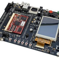
EA-OEM-204
Manufacturer Part Number
EA-OEM-204
Description
MCU, MPU & DSP Development Tools LPC2478-16 OEM BRD OEM BASE BRD W/TOUCH
Manufacturer
Embedded Artists
Specifications of EA-OEM-204
Processor To Be Evaluated
LPC2478
Data Bus Width
16 bit
Interface Type
RS-232, Ethernet, USB, I2C, SPI, UART
Core
ARM7TDMI-S
Dimensions
240 mm x 150 mm
Maximum Operating Temperature
+ 85 C
Operating Supply Voltage
3.3 V
Lead Free Status / RoHS Status
Lead free / RoHS Compliant


NXP Semiconductors
Table 4.
LPC2478
Product data sheet
Symbol
P0[23]/AD0[0]/
I2SRX_CLK/
CAP3[0]
P0[24]/AD0[1]/
I2SRX_WS/
CAP3[1]
P0[25]/AD0[2]/
I2SRX_SDA/
TXD3
P0[26]/AD0[3]/
AOUT/RXD3
P0[27]/SDA0
P0[28]/SCL0
P0[29]/USB_D+1
P0[30]/USB_D−1
P0[31]/USB_D+2
P1[0] to P1[31]
P1[0]/
ENET_TXD0
P1[1]/
ENET_TXD1
P1[2]/
ENET_TXD2/
MCICLK/
PWM0[1]
Pin description
Pin
18
16
14
12
50
48
61
62
51
196
194
185
[2]
[2]
[2]
[2][3]
[4]
[4]
[5]
[5]
[5]
[1]
[1]
[1]
…continued
Ball
H1
G2
F1
E1
T1
R3
U4
R6
T2
A3
B5
D9
[2]
[4]
[5]
[2][3]
[1]
[1]
[2]
[2]
[4]
[5]
[5]
[1]
All information provided in this document is subject to legal disclaimers.
Type
I/O
I
I/O
I
I/O
I
I/O
I
I/O
I
I/O
O
I/O
I
O
I
I/O
I/O
I/O
I/O
I/O
I/O
I/O
I/O
I/O
I/O
I/O
I/O
O
I/O
O
I/O
O
O
O
Rev. 2 — 29 September 2010
Description
P0[23] — General purpose digital input/output pin.
AD0[0] — A/D converter 0, input 0.
I2SRX_CLK — Receive Clock. It is driven by the master and received by
the slave. Corresponds to the signal SCK in the I
CAP3[0] — Capture input for Timer 3, channel 0.
P0[24] — General purpose digital input/output pin.
AD0[1] — A/D converter 0, input 1.
I2SRX_WS — Receive Word Select. It is driven by the master and
received by the slave. Corresponds to the signal WS in the I
specification.
CAP3[1] — Capture input for Timer 3, channel 1.
P0[25] — General purpose digital input/output pin.
AD0[2] — A/D converter 0, input 2.
I2SRX_SDA — Receive data. It is driven by the transmitter and read by
the receiver. Corresponds to the signal SD in the I
TXD3 — Transmitter output for UART3.
P0[26] — General purpose digital input/output pin.
AD0[3] — A/D converter 0, input 3.
AOUT — D/A converter output.
RXD3 — Receiver input for UART3.
P0[27] — General purpose digital input/output pin. Output is open-drain.
SDA0 — I
compliance).
P0[28] — General purpose digital input/output pin. Output is open-drain.
SCL0 — I
compliance).
P0[29] — General purpose digital input/output pin.
USB_D+1 — USB port 1 bidirectional D+ line.
P0[30] — General purpose digital input/output pin.
USB_D−1 — USB port 1 bidirectional D− line.
P0[31] — General purpose digital input/output pin.
USB_D+2 — USB port 2 bidirectional D+ line.
Port 1: Port 1 is a 32 bit I/O port with individual direction controls for each
bit. The operation of port 1 pins depends upon the pin function selected
via the pin connect block.
P1[0] — General purpose digital input/output pin.
ENET_TXD0 — Ethernet transmit data 0 (RMII/MII interface).
P1[1] — General purpose digital input/output pin.
ENET_TXD1 — Ethernet transmit data 1 (RMII/MII interface).
P1[2] — General purpose digital input/output pin.
ENET_TXD2 — Ethernet transmit data 2 (MII interface).
MCICLK — Clock output line for SD/MMC interface.
PWM0[1] — Pulse Width Modulator 0, output 1.
2
2
C0 clock input/output. Open-drain output (for I
C0 data input/output. Open-drain output (for I
Single-chip 16-bit/32-bit microcontroller
2
S-bus specification.
2
S-bus specification.
LPC2478
© NXP B.V. 2010. All rights reserved.
2
2
C-bus
C-bus
2
S-bus
13 of 91
Related parts for EA-OEM-204
Image
Part Number
Description
Manufacturer
Datasheet
Request
R

Part Number:
Description:
BOARD OEM W/LPC2478 MCU
Manufacturer:
Embedded Artists
Datasheet:
Part Number:
Description:
Development Boards & Kits - ARM LPC4357 OEM Board
Manufacturer:
Embedded Artists

Part Number:
Description:
MCU, MPU & DSP Development Tools LPC2468 OEM BRD OEM BASE BRD BUNDLE
Manufacturer:
Embedded Artists
Part Number:
Description:
KIT LPC3152 SODIMM 66X48 200POS
Manufacturer:
Embedded Artists
Datasheet:
Part Number:
Description:
KIT LPC3250 259 WITH QVGA
Manufacturer:
Embedded Artists
Datasheet:

Part Number:
Description:
Microcontroller Modules & Accessories LPC3250
Manufacturer:
Embedded Artists

Part Number:
Description:
Microcontroller Modules & Accessories LPC2478-16 BIT
Manufacturer:
Embedded Artists

Part Number:
Description:
Microcontroller Modules & Accessories LPC2478-32 BIT
Manufacturer:
Embedded Artists
Part Number:
Description:
Daughter Cards & OEM Boards LPC4088 OEM BOARD SODIMM
Manufacturer:
Embedded Artists
Datasheet:
Part Number:
Description:
KIT LPC3141 SODIMM 66X48 200POS
Manufacturer:
Embedded Artists
Datasheet:

Part Number:
Description:
MCU, MPU & DSP Development Tools LPC3131 BUNDLE W/O CODEC AND ETHERNET
Manufacturer:
Embedded Artists

Part Number:
Description:
MCU, MPU & DSP Development Tools LPC3131 KIT
Manufacturer:
Embedded Artists
Part Number:
Description:
KIT DEV LPC1788-32
Manufacturer:
Embedded Artists
Datasheet:
Part Number:
Description:
Microcontroller Modules & Accessories LPC3152
Manufacturer:
Embedded Artists
Part Number:
Description:
Microcontroller Modules & Accessories LPC3141
Manufacturer:
Embedded Artists