TFDU6103-TT3 Vishay, TFDU6103-TT3 Datasheet - Page 4
TFDU6103-TT3
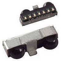
Manufacturer Part Number
TFDU6103-TT3
Description
Infrared Transceivers SIR 115.2kbits Top View
Manufacturer
Vishay
Datasheet
1.TFDU6103-TR3.pdf
(13 pages)
Specifications of TFDU6103-TT3
Data Rate Max
4Mbps
Data Transmission Distance
1m
Peak Wavelength
886nm
Supply Current
2mA
Supply Voltage Range
2.4V To 5.5V
Operating Temperature Range
-25°C To +85°C
Msl
MSL 4 - 72 Hours
Data Rate
4Mbs (FIR)
Idle Current, Typ @ 25° C
2mA
Link Range, Low Power
1m
Operating Temperature
-25°C ~ 85°C
Orientation
Top View
Shutdown
*
Size
9.7mm x 4.7mm x 4mm
Standards
IrPHY 1.4
Supply Voltage
2.4 V ~ 5.5 V
Lead Free Status / RoHS Status
Lead free / RoHS Compliant
Lead Free Status / RoHS Status
Lead free / RoHS Compliant, Lead free / RoHS Compliant
Available stocks
Company
Part Number
Manufacturer
Quantity
Price


TFDU6103
Vishay Semiconductors
Note
(1)
(2)
www.vishay.com
4
ELECTRICAL CHARACTERISTICS
PARAMETER
TRANSCEIVER
Input voltage high
(TXD, SD)
Input leakage current
(TXD, SD)
Input capacitance, TXD, SD
Output voltage low
Output voltage high
Output RXD current limitation
high state
low state
SD shutdown pulse duration
RXD to V
SD mode programming pulse
duration
OPTOELECTRONIC CHARACTERISTICS
PARAMETER
RECEIVER
Minimum irradiance E
angular range
Minimum irradiance E
angular range, MIR mode
Minimum irradiance E
inangular range, FIR mode
Maximum irradiance E
angular range
Maximum no detection
irradiance
Rise time of output signal
Fall time of output signal
RXD pulse width of output
signal, 50 %, SIR mode
RXD pulse width of output
signal, 50 %, MIR mode
RXD pulse width of output
signal, 50 %, FIR mode
Stochastic jitter, leading edge
Receiver start up time
Latency
T
Typical values are for design aid only, not guaranteed nor subject to production testing.
The typical threshold level is 0.5 x V
current.
amb
= 25 °C, V
CC1
impedance
(3)
(4)
CC1
SIR mode
= V
e
e
e
e
in
in
in
CC2
irdasupportAM@vishay.com, irdasupportAP@vishay.com,
= 2.4 V to 5.5 V unless otherwise noted.
For technical questions within your region, please contact one of the following:
Input irradiance = 100 mW/m
Input irradiance = 100 mW/m
After completion of shutdown programming
Input pulse length, 1.4 µs < P
Input pulse length, 1.4 µs < P
I
Input irradiance = 100 mW/m
I
CC1
OL
OH
Input irradiance = 100 mW/m
Input pulse length, P
Input pulse length, P
Input pulse length, P
TEST CONDITIONS
= 500 µA, C
Activating shutdown
= 250 µA, C
(V
Fast Infrared Transceiver Module (FIR, 4 Mbit/s)
V
Short to ground
CMOS level
CC1
IN
Short to V
sequence power on delay
9.6 kbit/s to 115.2 kbit/s
All modes
= 0.9 x V
= 850 nm to 900 nm
- 25 °C < T < 85 °C
= 850 nm to 900 nm
= 850 nm to 900 nm
= 850 nm to 900 nm
TEST CONDITIONS
10 % to 90 %, 15 pF
90 % to 10 %, 15 pF
= 3 V). It is recommended to use the specified min./max. values to avoid increased operating
1.152 Mbit/s
1.152 Mbit/s
(1)
load
load
4 Mbit/s
4 Mbit/s
4 Mbit/s
CC1
CC1
(2)
= 15 pF
(2)
= 15 pF
for 2.4 V to 5.5 V Operation
Wopt
Wopt
Wopt
(1)
2
2
, 115.2 kbit/s
= 217 ns,
= 125 ns,
= 250 ns,
, 1.152 Mbit/s
Wopt
2
Wopt
(5)
2
, 576 kbit/s
, 4 Mbit/s
< 25 µs,
< 25 µs
SYMBOL
t
R
SDPW
V
I
V
V
ICH
C
RXD
OH
OL
IH
I
irdasupportEU@vishay.com
SYMBOL
t
t
r (RXD)
f (RXD)
t
t
t
t
t
0.9 x V
E
E
E
E
E
PW
PW
PW
PW
PW
V
t
L
e
e
e
e
e
CC
MIN.
400
200
- 1
30
- 0.3
CC1
MIN.
(0.4)
110
100
225
1.5
10
10
4
TYP.
500
TYP.
(500)
(2.5)
(6.5)
250
2.1
1.8
(8)
25
65
80
40
5
Document Number: 81211
MAX.
600
+ 1
0.4
20
20
6
5
MAX.
(3.5)
270
140
275
350
250
100
2.6
Rev. 1.4, 29-Jul-09
(9)
35
90
40
40
20
40
80
(mW/cm
(µW/cm
(µW/cm
(µW/cm
(µW/cm
mW/m
mW/m
mW/m
mW/m
kW/m
UNIT
UNIT
mA
mA
µA
pF
k
µs
ns
V
V
V
ns
ns
µs
µs
ns
ns
ns
ns
ns
ns
ns
µs
µs
2
2
2
2
2
2
2
2
2
2
)
)
)
)
)
Related parts for TFDU6103-TT3
Image
Part Number
Description
Manufacturer
Datasheet
Request
R

Part Number:
Description:
Manufacturer:
Vishay Semiconductors
Datasheet:

Part Number:
Description:
Infrared Transceivers SIR 115.2kbits Side View
Manufacturer:
Vishay
Datasheet:

Part Number:
Description:
357-036-542-201 CARDEDGE 36POS DL .156 BLK LOPRO
Manufacturer:
Vishay
Datasheet:
Part Number:
Description:
357-036-542-201 CARDEDGE 36POS DL .156 BLK LOPRO
Manufacturer:
Vishay
Datasheet:
Part Number:
Description:
357-036-542-201 CARDEDGE 36POS DL .156 BLK LOPRO
Manufacturer:
Vishay
Datasheet:
Part Number:
Description:
357-036-542-201 CARDEDGE 36POS DL .156 BLK LOPRO
Manufacturer:
Vishay
Datasheet:
Part Number:
Description:
357-036-542-201 CARDEDGE 36POS DL .156 BLK LOPRO
Manufacturer:
Vishay
Datasheet:
Part Number:
Description:
357-036-542-201 CARDEDGE 36POS DL .156 BLK LOPRO
Manufacturer:
Vishay
Datasheet:
Part Number:
Description:
357-036-542-201 CARDEDGE 36POS DL .156 BLK LOPRO
Manufacturer:
Vishay
Datasheet:
Part Number:
Description:
357-036-542-201 CARDEDGE 36POS DL .156 BLK LOPRO
Manufacturer:
Vishay
Datasheet:
Part Number:
Description:
357-036-542-201 CARDEDGE 36POS DL .156 BLK LOPRO
Manufacturer:
Vishay
Datasheet:
Part Number:
Description:
357-036-542-201 CARDEDGE 36POS DL .156 BLK LOPRO
Manufacturer:
Vishay
Datasheet:
Part Number:
Description:
357-036-542-201 CARDEDGE 36POS DL .156 BLK LOPRO
Manufacturer:
Vishay
Datasheet:
Part Number:
Description:
357-036-542-201 CARDEDGE 36POS DL .156 BLK LOPRO
Manufacturer:
Vishay
Datasheet:
Part Number:
Description:
357-036-542-201 CARDEDGE 36POS DL .156 BLK LOPRO
Manufacturer:
Vishay
Datasheet: