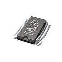
PCF8566TD NXP Semiconductors, PCF8566TD Datasheet - Page 7

PCF8566TD
Manufacturer Part Number
PCF8566TD
Description
LCD Drivers 96 SGMT LCD SGMT DRV
Manufacturer
NXP Semiconductors
Datasheet
1.PCF8566P112.pdf
(48 pages)
Specifications of PCF8566TD
Number Of Digits
12
Number Of Segments
96
Maximum Clock Frequency
315 KHz
Operating Supply Voltage
2.5 V to 6 V
Maximum Power Dissipation
400 mW
Package / Case
VSO-40
Maximum Supply Current
90 uA
Lead Free Status / RoHS Status
Lead free / RoHS Compliant
Other names
PCF8566T/1,112
NXP Semiconductors
PCF8566_7
Product data sheet
7.1 Power-on reset
7.2 LCD bias generator
7.3 LCD voltage selector
At power-on the PCF8566 resets to the following starting conditions:
Do not transfer data on the I
action to complete.
The full-scale LCD voltage (V
temperature compensated externally through the V
Fractional LCD biasing voltages are obtained from an internal voltage divider comprising
three series resistors connected between V
switched out of the circuit to provide a
configuration.
The LCD voltage selector coordinates the multiplexing of the LCD in accordance with the
selected LCD drive configuration. The operation of the voltage selector is controlled by
mode-set commands from the command decoder. The biasing configurations that apply to
the preferred modes of operation, together with the biasing characteristics as functions of
V
Fig 4. Typical system configuration
•
•
•
•
•
•
•
LCD
All backplane outputs are set to V
All segment outputs are set to V
Drive mode 1:4 multiplex with
Blinking is switched off
Input and output bank selectors are reset (as defined in
The I
The data pointer and the subaddress counter are cleared
and the resulting discrimination ratios (D), are given in
V
V
DD
SS
2
C-bus interface is initialized
CONTROLLER
PROCESSOR/
MICRO-
MICRO-
HOST
R
2 C
Rev. 07 — 25 February 2009
t
rise
bus
2
C-bus after a power-on for at least 1 ms to allow the reset
oper
) is obtained from V
OSC
SDA
1
SCL
3
DD
bias is selected
DD
1
2
6
1
7
2
A0
5
bias voltage level for the 1:2 multiplex
Universal LCD driver for low multiplex rates
V
8
DD
DD
PCF8566
A1
and V
9
A2
12
V
10
17 to 40
13 to 16
LCD
LCD
SA0
DD
LCD
11
supply to pin 12.
V
. The center resistor can be
SS
V
24 segment drives
LCD
4 backplanes
Table
Table
. The LCD voltage may be
8)
5.
PCF8566
© NXP B.V. 2009. All rights reserved.
LCD PANEL
(up to 96
elements)
mgg385
7 of 48


