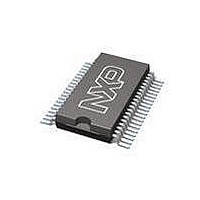
PCF8566TD NXP Semiconductors, PCF8566TD Datasheet - Page 29

PCF8566TD
Manufacturer Part Number
PCF8566TD
Description
LCD Drivers 96 SGMT LCD SGMT DRV
Manufacturer
NXP Semiconductors
Datasheet
1.PCF8566P112.pdf
(48 pages)
Specifications of PCF8566TD
Number Of Digits
12
Number Of Segments
96
Maximum Clock Frequency
315 KHz
Operating Supply Voltage
2.5 V to 6 V
Maximum Power Dissipation
400 mW
Package / Case
VSO-40
Maximum Supply Current
90 uA
Lead Free Status / RoHS Status
Lead free / RoHS Compliant
Other names
PCF8566T/1,112
NXP Semiconductors
Table 19.
V
[1]
[2]
[3]
[4]
PCF8566_7
Product data sheet
Symbol
LCD outputs
V
V
Z
SS
Fig 20. Normal mode
BP
S
o
= 0 V; V
Outputs open; inputs at V
Resets all logic when V
Periodically sampled, not 100 % tested.
Outputs measured one at a time.
( A)
I
DD
40
30
20
10
0
0
V
LCD
Static characteristics
DD
= 2.5 V to 6.0 V; V
= 0 V; f
11.1 Typical supply current characteristics
Parameter
voltage on pin BP
voltage on pin S
output impedance
2
clk(ext)
DD
= 200 kHz.
SS
< V
or V
4
POR
DD
LCD
.
…continued
; external clock with 50 % duty factor; I
= V
+85 C
40 C
6
DD
V
DD
mgg397
2.5 V to V
(V)
Rev. 07 — 25 February 2009
8
Conditions
BP0 to BP3;
C
S0 to S23;
C
on pin BP0 to BP3;
V
on pin S0 to S23;
V
DD
LCD
LCD
bpl
sgm
= 35 nF
= 5 nF
= V
= V
6.0 V; T
Fig 21. Low power mode
DD
DD
( A)
I
DD
amb
5 V
5 V
2
24
16
C-bus inactive.
8
0
Universal LCD driver for low multiplex rates
0
V
= 40 C to +85 C; unless otherwise specified.
LCD
[4]
[4]
= 0 V; f
Min
-
-
-
-
2
clk(ext)
= 35 kHz.
4
Typ
1
3
20
20
+85 C
40 C
6
PCF8566
© NXP B.V. 2009. All rights reserved.
V
Max
-
-
5
7
DD
mgg398
(V)
8
29 of 48
Unit
mV
mV
k
k


