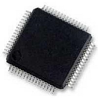
HV633PG-G Supertex, HV633PG-G Datasheet

HV633PG-G
Specifications of HV633PG-G
Related parts for HV633PG-G
HV633PG-G Summary of contents
Page 1
... Electroluminescent Displays ► Polycholesteric Displays Functional Block Diagram CSO Supertex inc. Gray-Shade Display Column Driver General Description The HV633 is a 32-channel driver IC for gray shade display use designed to produce varying output voltages between 3.0 - 80V. This amplitude modulation at the output is facilitated by an external ramp voltage V detailed explanation ...
Page 2
... CTL PP V High voltage supply PP V Ramp voltage R f Shift clock operating frequency ( Supertex inc. 0.80mm pitch 3.90mm footprint HV633PG-G Pin Configuration Value -0.5V to +7.5V -0.5V to +90V -0. +0.5V DD 1.5A 2.0W 2 125°C -65°C to +150°C Product Marking 260°C Package may or may not include the following marks ...
Page 3
... DH t Data-in pulse width WD t Load count pulse width WLC t Load count to ramp delay DLCR t Ramp to count clock delay 3 DRCC t Shift clock to load count delay time DSL Supertex inc. (over recommended operating conditions at T Min Typ - - - - -1.0 - -2.0 2 See performance curves ...
Page 4
... HV 1 OUT OUT Load shift register X X Load counter X X Counting/voltage X X conversion Notes Low logic level H = High logic level = Low to high transition = Transition of both edges X = Don’t care Supertex inc. Min Typ 10.6 2.0 3.0 = 80V. R bias current, typical CTL BIAS ...
Page 5
... SC = Shift Clock Load Count Count Clock, CSI = Chip Select Input, CSO = Chip Select Output *Data rate = 2x the SC frequency Output Stage Detail Internal 1 VCTL Logic & HV OUT Bias RCTL Circuit Q 2 Supertex inc. 7 L/E Data Latches Comparators 7 L/E Data Latches Comparators ● ● ● ● ● ● ● ● ● ● ...
Page 6
... Output source current can be calculated by using V Typical Panel Connections DIR = LOW VR, VPP LVGND, HVGND, SC, LC, CC, CSO VR, VPP LVGND, HVGND, SC, LC, CC, CSI DIR = HIGH Supertex inc. ). For gray shade #1 (000 0000). AOH VR HV633 + – Output Logic Stage LVGND HVGND (slew rate = 4.1V/µs) R /1.0KΩ ...
Page 7
... Chip Select Input (CSI Shift Clock SC1 (SC) Data DATA DATA (D1-D7) SET 1 SET Load Count (LC) Count Clock (CC) VR Supertex inc Load Load First Second Device Device ↑ ↓ ↑ ↓ ↑ ↓ ↑ ↓ ↑ ↓ ↑ ↑ ↓ ↓ ↑ ...
Page 8
... Typical Performance Curves Source Output Characteristics Volts GS Supertex inc. Gray Scale Voltage • • • • • • • • • • • • ...
Page 9
... The buses may of course be separate, and data can be strobed interleaved basis, etc., but those complica- tions will be left to systems designers. Supertex inc. When data has been loaded into all 32 outputs of all chips (top and bottom of the display panel), the load count pin is pulsed ...
Page 10
... LVGND 28 DIR * Analog VDD and digital VDD may be connected seperately for better noise immunity. Supertex inc. Description High-voltage outputs This is ground for the high-voltage (output) section. HVGND and LVGND should be connected together externally. High voltage ramp input for charging the output stage hold capacitors (CH). This input can be linear or non-linear as desired ...
Page 11
... OUT OUT * Analog VDD and digital VDD may be connected seperately for better noise immunity. Supertex inc. Description Low-voltage digital supply voltage. Inputs for binary-format parallel data. No connect. This is ground for the logic section. HVGND and LVGND should be connected together externally. No connect. ...
Page 12
... Pin Descriptions (cont.) Pin # Function OUT OUT OUT OUT OUT OUT Supertex inc. Description High-voltage outputs ● 1235 Bordeaux Drive, Sunnyvale, CA 94089 12 ● Tel: 408-222-8888 ● www.supertex.com HV633 ...
Page 13
... Drawings not to scale. Supertex Doc. #: DSPD-64PQFPPG, Version NR090608. (The package drawing(s) in this data sheet may not reflect the most current specifications. For the latest package outline information go to http://www.supertex.com/packaging.html.) does not recommend the use of its products in life support applications, and will not knowingly sell them for use in such applications unless it receives Supertex inc. an adequate “ ...


