CDB42L52 Cirrus Logic Inc, CDB42L52 Datasheet - Page 14
CDB42L52
Manufacturer Part Number
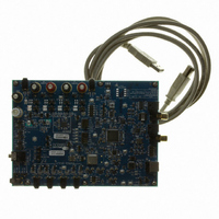
CDB42L52
Description
Eval Bd LP Codec W/Class D Spkr Driver
Manufacturer
Cirrus Logic Inc
Specifications of CDB42L52
Main Purpose
Audio, CODEC
Embedded
Yes, FPGA / CPLD
Utilized Ic / Part
CS42L52
Primary Attributes
4 Stereo Audio Inputs, Stereo Line and Speaker Outputs, S/PDIF Inputs and Outputs
Secondary Attributes
GUI, I2C, SPI, USB Interfaces
Description/function
Audio CODECs
Operating Supply Voltage
5 V
Product
Audio Modules
Lead Free Status / RoHS Status
Contains lead / RoHS non-compliant
For Use With/related Products
CS42L52
Lead Free Status / RoHS Status
Contains lead / RoHS non-compliant
Other names
598-1505


14
JMP
J31
J36
J25
J28
J52
J47
J74
J53
J48
J39
J38
J46
J49
J51
J13
J16
J11
J20
J14
J17
J12
J23
J15
J19
J7
SPKRB+-_FLT/NOFLT
SPKRA+_FLT/NOFLT
SPKRA-_FLT/NOFLT
SPKRB-_FLT/NOFLT
SPKR_A+_CONN
SPKR_B+_CONN
SPKR_A-_CONN
SPKR_B-_CONN
AIN1A_AC_DC
AIN1A_AC_DC
MIC1+_BIAS
MIC2+_BIAS
MIC1-_BIAS
MIC2-_BIAS
LABEL
+VA_HP
VA_HP
MONO
MONO
VD
VD
VP
VL
VA
VL
VA
Selects either AC or DC couple for
Selects either AC or DC couple for
Selects MICBIAS for MIC1+ Input
Selects MICBIAS for MIC2+ Input
Selects MICBIAS for MIC1- Input
Selects MICBIAS for MIC1- Input
Selects Full or Half Bridge output
Selects Full or Half Bridge output
Selects FLT or NOFLT output for
Selects FLT or NOFLT output for
Selects FLT or NOFLT output for
Selects FLT or NOFLT output for
Selects source of voltage for the
Selects source of voltage for the
Selects source of voltage for the
Selects source of voltage for the
Selects LCFLT or RCFLT output
Selects LCFLT or RCFLT output
Selects LCFLT or RCFLT output
Selects LCFLT or RCFLT output
Current Measurement
for SPKOUTB-/+
for SPKOUTA-/+
for SPKOUTB+
for SPKOUTA+
for SPKOUTB-
VA_HP supply
for SPKOUTA-
PURPOSE
AIN1A Input
AIN1B Input
SPKOUTA+
SPKOUTB+
SPKOUTA-
SPKOUTB-
VD supply
VL supply
VA supply
Table 2. Jumper Settings
POSITION
*SHUNTED
SHUNTED
SHUNTED
SHUNTED
SHUNTED
SHUNTED
SHUNTED
SHUNTED
SHUNTED
*OPEN
*OPEN
*OPEN
*OPEN
*OPEN
*OPEN
*OPEN
*OPEN
*+1.8V
*+1.8V
*+1.8V
*+1.8V
OPEN
+2.5V
+3.3V
+2.5V
+2.5V
+2.5V
*2 - 3
*2 - 3
*2 - 3
*2 - 3
*2 - 3
*2 - 3
*2 - 3
*2 - 3
1 - 2
1 - 2
1 - 2
1 - 2
1 - 2
1 - 2
1 - 2
1 - 2
Voltage source is +1.8 V regulator.
Voltage source is +2.5 V regulator.
Voltage source is +3.3 V regulator.
Voltage source is +1.8 V regulator.
Voltage source is +2.5 V regulator. .
Voltage source is +1.8 V regulator.
Voltage source is +2.5 V regulator. .
Voltage source is +1.8 V regulator.
Voltage source is +2.5 V regulator. .
1 Ω series resistor is shorted.
1 Ω series resistor in power supply path.
AIN1A input is AC coupled to ADC.
AIN1A input is DCcoupled to ADC.
AIN1A input is AC coupled to ADC.
AIN1A input is DCcoupled to ADC.
AIN3A/MIC1- Input from Audio Jack.
AIN3A/MIC1- Input is MICBIAS.
AIN3B/MIC2- Input from Audio Jack.
AIN3B/MIC2- Input is MICBIAS.
AIN4A/MIC1+ Input from Audio Jack.
AIN4A/MIC1+ Input is MICBIAS.
AIN4B/MIC2+ Input from Audio Jack.
AIN4B/MIC2+ Input is MICBIAS.
No filtered output selected for SPKOUTA-.
LC filtered output selected for SPKOUTA-.
No filtered output selected for SPKOUTA+.
LC filtered output selected for SPKOUTA+.
No filtered output selected for SPKOUTB-.
LC filtered output selected for SPKOUTB-.
No filtered output selected for SPKOUTB+.
LC filtered output selected for SPKOUTB+.
RC filtered SPKOUTA- to J6.
LC filtered SPKOUTA- to J6 and J60.
RC filtered SPKOUTA+ to J6.
LC filtered SPKOUTA+ to J6 and J59.
RC filtered SPKOUTB- to J18.
LC filtered SPKOUTB- to J18 and J101.
RC filtered SPKOUTB+ to J18.
LC filtered SPKOUTB+ to J18 and J99.
Stereo Full Bridge outputs to J60 and J59.
Mono Full Bridge output to J60 and J59.
Stereo Full Bridge outputs to J101 and J99.
Mono Full Bridge output to J101 and J99.
FUNCTION SELECTED
CDB42L52
DS680DB1
Related parts for CDB42L52
Image
Part Number
Description
Manufacturer
Datasheet
Request
R

Part Number:
Description:
Development Kit
Manufacturer:
Cirrus Logic Inc
Datasheet:
Part Number:
Description:
Development Kit
Manufacturer:
Cirrus Logic Inc
Datasheet:


Part Number:
Description:
High-efficiency PFC + Fluorescent Lamp Driver Reference Design
Manufacturer:
Cirrus Logic Inc
Datasheet:
Part Number:
Description:
Development Kit
Manufacturer:
Cirrus Logic Inc
Datasheet:
Part Number:
Description:
Development Kit
Manufacturer:
Cirrus Logic Inc
Datasheet:

Part Number:
Description:
Development Kit
Manufacturer:
Cirrus Logic Inc
Datasheet:
Part Number:
Description:
Development Kit
Manufacturer:
Cirrus Logic Inc
Datasheet:
Part Number:
Description:
Development Kit
Manufacturer:
Cirrus Logic Inc
Datasheet:
Part Number:
Description:
Development Kit
Manufacturer:
Cirrus Logic Inc
Datasheet:

Part Number:
Description:
EVALUATION BOARD FOR CS8427
Manufacturer:
Cirrus Logic Inc
Datasheet:

Part Number:
Description:
BOARD EVAL FOR CS8416 RCVR
Manufacturer:
Cirrus Logic Inc
Datasheet:

Part Number:
Description:
EVALUATION BOARD FOR CS8420
Manufacturer:
Cirrus Logic Inc
Datasheet:

Part Number:
Description:
KIT DEVELOPMENT EP9315 ARM9
Manufacturer:
Cirrus Logic Inc
Datasheet:

Part Number:
Description:
KIT DEVELOPMENT EP9302 ARM9
Manufacturer:
Cirrus Logic Inc
Datasheet: