GT10Q101 Toshiba, GT10Q101 Datasheet

IGBT, 1200V, TO-3P(N)

GT10Q101

Manufacturer Part Number
GT10Q101
Description
IGBT, 1200V, TO-3P(N)
Manufacturer
Toshiba
Datasheets

Specifications of GT10Q101

Transistor Type
IGBT
Dc Collector Current
10A
Collector Emitter Voltage Vces
2.7V
Power Dissipation Max
140W
Collector Emitter Voltage V(br)ceo
1.2kV
Transistor Case Style
TO-3P
No. Of Pins
3
Current Ic
RoHS Compliant
Channel Type
N
Configuration
Single
Collector-emitter Voltage
1.2kV
Gate To Emitter Voltage (max)
±20V
Package Type
TO-3PN
Pin Count
3 +Tab
Mounting
Through Hole
Operating Temperature (max)
150C
Operating Temperature Classification
Military
Power Dissipation Pd
140W
Rohs Compliant
Yes
Svhc
No SVHC
Lead Free Status / Rohs Status
Not Compliant
High Power Switching Applications
Absolute Maximum Ratings
Marking
Third-generation IGBT
Enhancement mode type
High speed: t
Low saturation voltage: V
Collector-emitter voltage
Gate-emitter voltage
Collector current
Collector power dissipation
(Tc = 25°C)
Junction temperature
Storage temperature range
Note: Using continuously under heavy loads (e.g. the application of high
temperature/current/voltage and the significant change in
temperature, etc.) may cause this product to decrease in the
reliability significantly even if the operating conditions (i.e.
operating temperature/current/voltage, etc.) are within the absolute maximum ratings.
Please design the appropriate reliability upon reviewing the Toshiba Semiconductor Reliability Handbook
(“Handling Precautions”/Derating Concept and Methods) and individual reliability data (i.e. reliability test report
and estimated failure rate, etc).
Characteristic
GT10Q101
TOSHIBA
f
= 0.32 µs (max)
1 ms
CE (sat)
DC
TOSHIBA Insulated Gate Bipolar Transistor Silicon N Channel IGBT
Part No. (or abbreviation code)
Lot No.
A line indicates
lead (Pb)-free package or
lead (Pb)-free finish.
= 2.7 V (max)
(Ta = 25°C)
Symbol
V
V
GT10Q101
T
I
P
GES
CES
I
CP
T
stg
C
C
j
−55~150
Rating
1200
±20
140
150
10
20
1
Unit
°C
°C
W
V
V
A
Weight: 4.6 g (typ.)
JEDEC
JEITA
TOSHIBA
2-16C1C
GT10Q101
2006-10-31
Unit: mm

Related parts for GT10Q101

GT10Q101 Summary of contents

Page 1

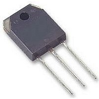
... Part No. (or abbreviation code) Lot No. A line indicates lead (Pb)-free package or lead (Pb)-free finish. GT10Q101 = 2.7 V (max) (Ta = 25°C) Symbol Rating Unit V 1200 V CES ± GES 140 150 °C j −55~150 T °C stg 1 GT10Q101 Unit: mm JEDEC ― JEITA ― TOSHIBA 2-16C1C Weight: 4.6 g (typ.) 2006-10-31 ...

Page 2

... Inductive Load t = 600 ± Ω off ⎯ ( (off) 10% 10 GT10Q101 Min Typ. ⎯ ⎯ ⎯ ⎯ ⎯ 4.0 ⎯ 2.1 ⎯ 600 ⎯ 0.07 ⎯ 0.30 ⎯ 0.16 (Note1) ⎯ 0.50 ⎯ ⎯ 10% 90% 90% 10% 10 (on off on 2006-10-31 Max Unit ± ...

Page 3

... Tc = 25° Gate-emitter voltage V ( – Common emitter 125°C − Gate-emitter voltage V ( Common emitter −40° Gate-emitter voltage V 20 Common emitter Tc = 125° Gate-emitter voltage V 4 Common emitter −60 −20 20 Case temperature Tc (°C) 3 GT10Q101 V – ( – ( – (sat 100 140 2006-10-31 ...

Page 4

... Switching loss Common emitter 600 ± Ω 25° 125°C Note2 0.5 0 off 0.1 E off 0.05 0.03 0.01 300 500 GT10Q101 Switching time – Common emitter 600 ± Ω 25° 125° Collector current I (A) C Switching time – I off ...

Page 5

... C ies 800 Tc = 25°C 600 C oes 400 C res 200 0 1000 0 ( μ 0 < = 125°C 0 ± Ω 0.1 1000 3000 1 3 (V) Collector-emitter voltage GT10Q101 – 600 400 200 100 Gate charge Q (nC) G Reverse bias SOA 10 30 100 300 1000 3000 (V) CE 2006-10-31 ...

Page 6

... Please contact your sales representative for product-by-product details in this document regarding RoHS compatibility. Please use these products in this document in compliance with all applicable laws and regulations that regulate the inclusion or use of controlled substances. Toshiba assumes no liability for damage or losses occurring as a result of noncompliance with applicable laws and regulations. 6 GT10Q101 20070701-EN 2006-10-31 ...

Related keywords