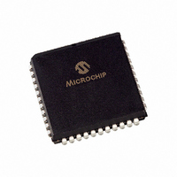
PIC18F448-I/L Microchip Technology, PIC18F448-I/L Datasheet - Page 245

PIC18F448-I/L
Manufacturer Part Number
PIC18F448-I/L
Description
IC,MICROCONTROLLER,8-BIT,PIC CPU,CMOS,LDCC,44PIN,PLASTIC
Manufacturer
Microchip Technology
Series
PIC® 18Fr
Datasheets
1.PIC18LF242-ISO.pdf
(36 pages)
2.PIC18F248-ISO.pdf
(402 pages)
3.PIC18F248-ISO.pdf
(8 pages)
Specifications of PIC18F448-I/L
Rohs Compliant
YES
Core Processor
PIC
Core Size
8-Bit
Speed
40MHz
Connectivity
CAN, I²C, SPI, UART/USART
Peripherals
Brown-out Detect/Reset, LVD, POR, PWM, WDT
Number Of I /o
33
Program Memory Size
16KB (8K x 16)
Program Memory Type
FLASH
Eeprom Size
256 x 8
Ram Size
768 x 8
Voltage - Supply (vcc/vdd)
4.2 V ~ 5.5 V
Data Converters
A/D 8x10b
Oscillator Type
External
Operating Temperature
-40°C ~ 85°C
Package / Case
44-PLCC
Processor Series
PIC18F
Core
PIC
Data Bus Width
8 bit
Data Ram Size
768 B
Interface Type
SPI, I2C, USART
Maximum Clock Frequency
40 MHz
Number Of Programmable I/os
33
Number Of Timers
4
Operating Supply Voltage
2 V to 5.5 V
Maximum Operating Temperature
+ 85 C
Mounting Style
SMD/SMT
3rd Party Development Tools
52715-96, 52716-328, 52717-734, 52712-325, EWPIC18
Development Tools By Supplier
PG164130, DV164035, DV244005, DV164005, PG164120, ICE2000, DV164136, DM163011
Minimum Operating Temperature
- 40 C
On-chip Adc
10 bit, 8 Channel
Lead Free Status / RoHS Status
Contains lead / RoHS non-compliant
For Use With
AC164309 - MODULE SKT FOR PM3 44PLCC444-1001 - DEMO BOARD FOR PICMICRO MCUDVA16XL441 - ADAPTER DEVICE ICE 44PLCCDV007003 - PROGRAMMER UNIVERSAL PROMATE II
Lead Free Status / Rohs Status
Details
Other names
PIC18F448I/L
Available stocks
Company
Part Number
Manufacturer
Quantity
Price
Company:
Part Number:
PIC18F448-I/L
Manufacturer:
Microchip Technology
Quantity:
10 000
- Current page: 245 of 402
- Download datasheet (7Mb)
The analog reference voltage is software selectable to
either the device’s positive and negative supply voltage
(V
V
The A/D converter has a unique feature of being able
to operate while the device is in Sleep mode. To oper-
ate in Sleep, the A/D conversion clock must be derived
from the A/D’s internal RC oscillator.
The output of the sample and hold is the input into the
converter which generates the result via successive
approximation.
FIGURE 20-1:
© 2006 Microchip Technology Inc.
REF
DD
+ pin and RA2/AN2/V
and V
Note 1: Channels AN5 through AN7 are not available on PIC18F2X8 devices.
SS
2: All I/O pins have diode protection to V
) or the voltage level on the RA3/AN3/
Converter
10-bit
A/D
Reference
voltage
A/D BLOCK DIAGRAM
REF
- pin.
V
V
REF
REF
-
+
(Input Voltage)
V
AIN
PCFG0
DD
and V
V
DD
A device Reset forces all registers to their Reset state.
This forces the A/D module to be turned off and any
conversion is aborted.
Each port pin associated with the A/D converter can be
configured as an analog input (RA3 can also be a
voltage reference) or as a digital I/O.
The ADRESH and ADRESL registers contain the result
of the A/D conversion. When the A/D conversion is com-
plete, the result is loaded into the ADRESH/ADRESL
registers, the GO/DONE bit (ADCON0<2>) is cleared
and A/D Interrupt Flag bit, ADIF, is set. The block
diagram of the A/D module is shown in Figure 20-1.
SS
.
V
SS
CHS2:CHS0
111
110
101
100
011
010
001
000
PIC18FXX8
DS41159E-page 243
AN7
AN2
AN1
AN0
AN6
AN5
AN4
AN3
(1)
(1)
(1)
Related parts for PIC18F448-I/L
Image
Part Number
Description
Manufacturer
Datasheet
Request
R

Part Number:
Description:
IC, 8BIT MCU, PIC18F, 40MHZ, LCC-44
Manufacturer:
Microchip Technology
Datasheet:

Part Number:
Description:
IC, 8BIT MCU, PIC18LF, 40MHZ, PLCC-64
Manufacturer:
Microchip Technology
Datasheet:

Part Number:
Description:
IC, 8BIT MCU, PIC18F, 64MHZ, TQFP-80
Manufacturer:
Microchip Technology
Datasheet:

Part Number:
Description:
MCU, MPU & DSP Development Tools CAN/LIN PICtail Plus Daughter Board
Manufacturer:
Microchip Technology
Datasheet:

Part Number:
Description:
IC, 8BIT MCU, PIC18F, 64MHZ, DIP-40
Manufacturer:
Microchip Technology
Datasheet:

Part Number:
Description:
IC, 8BIT MCU, PIC18LF, 40MHZ, PLCC-64
Manufacturer:
Microchip Technology
Datasheet:

Part Number:
Description:
IC, 8BIT MCU, PIC18F, 64MHZ, TQFP-64
Manufacturer:
Microchip Technology

Part Number:
Description:
IC, 8BIT MCU, PIC18F, 64MHZ, TQFP-80
Manufacturer:
Microchip Technology

Part Number:
Description:
8KB, Flash, 768bytes-RAM, 36I/O, 8-bit Family,nanowatt XLP 40 UQFN 5x5x0.5mm TUB
Manufacturer:
Microchip Technology
Datasheet:

Part Number:
Description:
8KB, Flash, 768bytes-RAM, 36I/O, 8-bit Family,nanowatt XLP 40 UQFN 5x5x0.5mm TUB
Manufacturer:
Microchip Technology

Part Number:
Description:
16KB, Flash, 768bytes-RAM, 36I/O, 8-bit Family,nanowatt XLP 40 UQFN 5x5x0.5mm TU
Manufacturer:
Microchip Technology
Datasheet:

Part Number:
Description:
16KB, Flash, 768bytes-RAM, 36I/O, 8-bit Family,nanowatt XLP 40 UQFN 5x5x0.5mm TU
Manufacturer:
Microchip Technology

Part Number:
Description:
32KB, Flash, 1536bytes-RAM, 36I/O, 8-bit Family,nanowatt XLP 40 UQFN 5x5x0.5mm T
Manufacturer:
Microchip Technology
Datasheet:

Part Number:
Description:
32KB, Flash, 1536bytes-RAM, 36I/O, 8-bit Family,nanowatt XLP 40 UQFN 5x5x0.5mm T
Manufacturer:
Microchip Technology

Part Number:
Description:
64KB, Flash, 3968bytes-RAM, 36I/O, 8-bit Family,nanowatt XLP 40 UQFN 5x5x0.5mm T
Manufacturer:
Microchip Technology
Datasheet:


