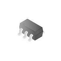
DG2020DV-T1-E3 Vishay, DG2020DV-T1-E3 Datasheet

DG2020DV-T1-E3
Specifications of DG2020DV-T1-E3
Related parts for DG2020DV-T1-E3
DG2020DV-T1-E3 Summary of contents
Page 1
... The switch conducts equally well in both directions when on, and blocks up to the power supply level when off. Logic 0 NO (Source ) 1 1 COM NC (Source ) 2 Temp Range - DG2020 Vishay Siliconix D Cellular Phones D Communication Systems D Portable Test Equipment D Battery Operated Systems OFF OFF ON Package Part Number TSOP-6 DG2020DV www.vishay.com 1 ...
Page 2
... DG2020 Vishay Siliconix Reference to GND IN, COM, NC Continuous Current (Any terminal Peak Current . . . . . . . . . . . . . . . . . . . . . . . . . . . . . . . . . . . . . . . . . . . . (Pulsed at 1 ms, 10% duty cycle) Storage Temperature (D Suffix Parameter Symbol Analog Switch Analog Signal Range r On-Resistance Flatness ON Flatness I f Switch Off Leakage Current I f Channel-On Leakage Current I Digital Control ...
Page 3
... 300 nF GEN GEN = pF MHz V MHz Vishay Siliconix Limits –40 to 85_C Min Typ Max e Temp Full 0 Room 0.8 Full 0.9 Room 1.2 Full 1.3 Room 0.13 Room –5.3 Full –98 Room –5.3 Full –98 Room –5.3 Full –98 Full 2.4 Full Full 3 ...
Page 4
... DG2020 Vishay Siliconix r vs. V and Supply Voltage ON COM 4.0 3.5 3.0 2 2.7 V (NC) 2 2.7 V (NO) 1.5 1.0 0.5 0 – Analog Voltage (V) COM r vs. Analog Voltage and Temperature ON 1. 85_C NC @ 25_C 1. –40_C 1. 85_C 0. 25_C 0. – Analog Voltage (V) COM Supply Current vs. Input Switching Frequency ...
Page 5
... OFF 100 Logic Input Switch Output V OUT Switch Output 300 FIGURE 1. Switching Time DG2020 Vishay Siliconix Insertion Loss, Off-Isolation Crosstalk vs. Frequency 10 LOSS –10 –30 –50 OIRR –70 X TALK –90 100 100 M Frequency (Hz) Charge Injection vs. Analog Voltage 20 NO Switch 10 0 – – – ...
Page 6
... DG2020 Vishay Siliconix COM GND C (includes fixture and stray capacitance gen COM + IN V gen – GND COM COM R L Analyzer V COM Off Isolation + 20 log FIGURE 3. Off-Isolation www.vishay.com 6 New Product Logic Input 300 Switch 0 V Output FIGURE 5. Break-Before-Make Interval OUT V OUT FIGURE 2. Charge Injection 10 nF 0V, 2 ...
Page 7
... Vishay disclaims any and all liability arising out of the use or application of any product described herein or of any information provided herein to the maximum extent permitted by law. The product specifications do not expand or otherwise modify Vishay’ ...


