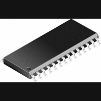
CS4360-KS Cirrus Logic Inc, CS4360-KS Datasheet - Page 25

CS4360-KS
Manufacturer Part Number
CS4360-KS
Description
D/A Converter (D-A) IC
Manufacturer
Cirrus Logic Inc
Datasheet
1.CS4360-KZZ.pdf
(37 pages)
Specifications of CS4360-KS
No. Of Pins
28
No. Of Bits
24 Bit
Mounting Type
Surface Mount
Interface Type
Serial
Package / Case
28-SOIC
Available stocks
Company
Part Number
Manufacturer
Quantity
Price
Part Number:
CS4360-KS EP
Manufacturer:
CIRRUS
Quantity:
20 000
Part Number:
CS4360-KSZ
Manufacturer:
CIRRUS
Quantity:
20 000
4.6.3
To prevent an audio transient at the next power-on, the DC-blocking capacitors must fully discharge be-
fore turning on the power or exiting the power-down state. If full discharge does not occur, a transient will
occur when the audio outputs are initially clamped to GND. The time that the device must remain in the
power-down state is related to the value of the DC-blocking capacitance and the output load. For example,
with a 3.3 µF capacitor, the minimum power-down time will be approximately 0.4 seconds.
4.7
The Mute Control pins go high during power-up initialization, reset, muting (see section 6.1.1 and 6.4.1),
or if the MCLK to LRCK ratio is incorrect. These pins are intended to be used as control for external mute
circuits to prevent the clicks and pops that can occur in any single-ended single supply system.
Use of the Mute Control function is not mandatory but recommended for designs requiring the absolute
minimum in extraneous clicks and pops. Also, use of the Mute Control function can enable the system
designer to achieve idle channel noise/signal-to-noise ratios which are only limited by the external mute
circuit. Please see the CDB4360 data sheet for a suggested mute circuit.
4.8
As with any high-resolution converter, the CS4360 requires careful attention to power supply and ground-
ing arrangements if its potential performance is to be realized. Figure 1 shows the recommended power
arrangements, with VA, VD, VLS and VLC connected to clean supplies. If the ground planes are split be-
tween digital ground and analog ground, the GND pins of the CS4360 should be connected to the analog
ground plane.
All signals, especially clocks, should be kept away from the FILT+ and VQ pins in order to avoid unwanted
coupling into the modulators. The CDB4360 evaluation board demonstrates the optimum layout and pow-
er supply arrangements.
4.8.1
Decoupling capacitors should be placed as close to the DAC as possible, with the low-value ceramic ca-
pacitor being the closest. To further minimize impedance, these capacitors should be located on the same
layer as the DAC. If desired, all supply pins may be connected to the same supply, but a decoupling ca-
pacitor should still be placed on each supply pin and referenced to analog ground.
4.8.2
Each power supply pin provides power to specific sections of the CS4360. The logic voltage level for each
section must adhere to the corresponding power supply voltage setting. For example: If VLC = 1.8 V; VLS
= 3.3 V; VD = VA = 5 V; then the logic level for all mode configuration inputs must equal 1.8 V.
4.9
The control port is used to load all the internal register settings (see section 6). The operation of the control
port may be completely asynchronous with the audio sample rate. However, to avoid potential interfer-
ence problems, the control port pins should remain static if no operation is required.
The control port operates in one of two modes: I²C or SPI.
Notes: MCLK must be applied during all I²C communication.
DS517F2
10, 11, 12, 13, 15
2, 3, 4, 5, 6, 7
Mute Control
Grounding and Power Supply Arrangements
Control Port Interface
Pin #s
Discharge Time
Capacitor Placement
Power Supply Sections
Serial Audio Interface Inputs
Mode Configuration Inputs
Table 7. Power Supply Control Sections
Description
Power Supply Reference
VLS
VLC
CS4360
25


