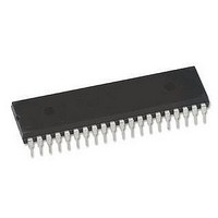
P89V51RC2FN NXP Semiconductors, P89V51RC2FN Datasheet - Page 66

P89V51RC2FN
Manufacturer Part Number
P89V51RC2FN
Description
IC, MCU 8BIT 80C51 32K FLASH, DIP40
Manufacturer
NXP Semiconductors
Datasheet
1.P89V51RC2FBC557.pdf
(80 pages)
Specifications of P89V51RC2FN
Controller Family/series
(8051) 8052
Core Size
8bit
No. Of I/o's
32
Program Memory Size
32KB
Ram Memory Size
1KB
Cpu Speed
33MHz
Oscillator Type
External Only
No. Of Timers
4
No. Of Pwm
RoHS Compliant
Package
40PDIP
Device Core
80C51
Family Name
89V
Maximum Speed
40 MHz
Ram Size
1 KB
Operating Supply Voltage
5 V
Data Bus Width
8 Bit
Program Memory Type
Flash
Number Of Programmable I/os
32
Interface Type
SPI/UART
Operating Temperature
-40 to 85 °C
Number Of Timers
3
Available stocks
Company
Part Number
Manufacturer
Quantity
Price
Company:
Part Number:
P89V51RC2FN
Manufacturer:
ST
Quantity:
9 576
NXP Semiconductors
P89V51RB2_RC2_RD2_5
Product data sheet
Fig 31. External program memory read cycle
PSEN
port 0
port 2
ALE
9.1 Explanation of symbols
Each timing symbol has 5 characters. The first character is always a ‘T’ (stands for time).
The other characters, depending on their positions, stand for the name of a signal or the
logical status of that signal. The following is a list of all the characters and what they stand
for.
A — Address
C — Clock
D — Input data
H — Logic level HIGH
I — Instruction (program memory contents)
L — Logic level LOW or ALE
P — PSEN
Q — Output data
R — RD signal
T — Time
V — Valid
W — WR signal
X — No longer a valid logic level
Z — High impedance (Float)
Example:
t
t
AVLL
LLPL
t
= Address valid to ALE LOW time
= ALE LOW to PSEN LOW time
AVLL
t
LHLL
t
LLAX
A0 to A7
Rev. 05 — 12 November 2009
t
LLPL
t AVIV
A8 to A15
t
PLAZ
t
t
PLIV
LLIV
INSTR IN
t
PXIX
t
PXIZ
P89V51RB2/RC2/RD2
t
PLPH
8-bit microcontrollers with 80C51 core
t
PXAV
A0 to A7
A8 to A15
002aaa548
© NXP B.V. 2009. All rights reserved.
66 of 80


