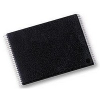
HY27UF084G2B-TPCB HYNIX SEMICONDUCTOR, HY27UF084G2B-TPCB Datasheet - Page 15

HY27UF084G2B-TPCB
Manufacturer Part Number
HY27UF084G2B-TPCB
Description
IC, MEMORY, FLASH NAND 4GB, TSOP48
Manufacturer
HYNIX SEMICONDUCTOR
Datasheet
1.HY27UF084G2B-TPCB.pdf
(51 pages)
Specifications of HY27UF084G2B-TPCB
Access Time
20ns
Supply Voltage Range
2.7V To 3.6V
Memory Case Style
TSOP
No. Of Pins
48
Operating Temperature Range
0°C To +70°C
Package / Case
TSOP
Base Number
27
Interface
Parallel
Logic
RoHS Compliant
Memory Type
Flash - NAND
Memory Configuration
512M X 8
Rohs Compliant
Yes
Available stocks
Company
Part Number
Manufacturer
Quantity
Price
Company:
Part Number:
HY27UF084G2B-TPCB
Manufacturer:
HYNIX
Quantity:
11 250
Company:
Part Number:
HY27UF084G2B-TPCB
Manufacturer:
HYNIX
Quantity:
12 500
Part Number:
HY27UF084G2B-TPCB
Manufacturer:
HYNIX/海力士
Quantity:
20 000
1
HY27UF(08/16)4G2B Series
4Gbit (512Mx8bit) NAND Flash
3.13 Cache Read
Cache read operation allows automatic download of consecutive pages. Immediately after 1st latency end, while user
can start reading out data, device internally starts reading following page.
Start address of 1st page is at page start (A<10:0>=00h), after 1st latency time (tr) , automatic data download will
be uninterrupted. In fact latency time is 25us, while download of a page require at least 100us for x8 device. (50us for
x16device).
The Cache Read function may be issued after the Read function is complete (SR[6] is set to one). The host may enter
the address of the next page to be read from the Flash array. Data output always begins at column address 00h. If
the host does not enter an address to retrieve, the next sequential page is read. When the Cache Read function is
issued, SR[6] is cleared to zero (busy). After the operation is begun SR[6] is set to one (ready) and the host may
begin to read the data from the previous Read or Cache Read function. Issuing an additional Cache Read function
copies the data most recently read from the array into the page register. When no more pages are to be read, the
final page is copied into the page register by issuing the 3Fh command. The host may begin to read data from the
page register when SR[6]is set to one (ready). When the 31h and 3Fh commands are issued, SR[6] shall be cleared
to zero (busy) until the page has finished being copied from the Flash array.
The host shall not issue a sequential Read Cache (31h) command after the last page of the device is read.
Refer to Figure 13.
Cache Read operation must be done only block by block if system needs to avoid reading also reading from invalid
blocks.
Rev 0.4 / Jan. 2008
15


