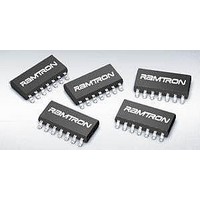
FM31L278-G Ramtron, FM31L278-G Datasheet - Page 21

FM31L278-G
Manufacturer Part Number
FM31L278-G
Description
FRAM, MPU SUPPORT, 256K, RTC, SOIC14
Manufacturer
Ramtron
Datasheet
1.FM31L272-G.pdf
(26 pages)
Specifications of FM31L278-G
Memory Size
256Kbit
Nvram Features
RTC
Supply Voltage Range
2.7V To 3.6V
Memory Case Style
SOIC
No. Of Pins
14
Operating Temperature Range
-40°C To +85°C
Package / Case
SOIC
Mounting Style
SMD/SMT
Memory Configuration
32768 X 8
Interface Type
I2C, Serial, 2-Wire
Rohs Compliant
Yes
Number Of Voltages Monitored
1
Monitored Voltage
2.6 V or 2.9 V
Output Type
Active Low, Open Drain
Manual Reset
Resettable
Watchdog
Watchdog
Battery Backup Switching
Yes
Power-up Reset Delay (typ)
200 ms
Supply Voltage (max)
3.6 V
Supply Voltage (min)
2.7 V
Supply Current (typ)
1500 uA
Power Fail Detection
Yes
Lead Free Status / RoHS Status
Lead free / RoHS Compliant
Lead Free Status / RoHS Status
Lead free / RoHS Compliant
Available stocks
Company
Part Number
Manufacturer
Quantity
Price
Part Number:
FM31L278-G
Manufacturer:
CYPRESS/赛普拉斯
Quantity:
20 000
Company:
Part Number:
FM31L278-GTR
Manufacturer:
SIEMENS
Quantity:
124
Part Number:
FM31L278-GTR
Manufacturer:
CYPRESS
Quantity:
20 000
Electrical Specifications
Absolute Maximum Ratings
* PFI input voltage must not exceed 4.5V.
** The “V
Stresses above those listed under Absolute Maximum Ratings may cause permanent damage to the device. This is a stress rating only,
and the functional operation of the device at these or any other conditions above those listed in the operational section of this
specification is not implied. Exposure to absolute maximum ratings conditions for extended periods may affect device reliability.
DC Operating Conditions
Rev. 2.0
Jan. 2011
Symbol
V
I
I
V
I
I
V
V
V
I
I
V
V
DD
SB
BAK
BAKTC
LI
LO
DD
BAK
TP1
TP2
RST
IL
IH
Symbol
T
V
IN
V
T
V
V
LEAD
BAK
STG
ESD
< V
DD
IN
Main Power Supply
V
Standby Current
RTC Backup Supply Voltage
RTC Backup Supply Current
Trickle Charge Current with V
V
V
V
Input Leakage Current
Output Leakage Current
Input Low Voltage
Input High Voltage
@ T
@ T
@ T
@ T
@ T
@ T
DD
@ SCL = 100 kHz
@ SCL = 400 kHz
@ SCL = 1 MHz
Fast Charge Off (FC = 0)
Fast Charge On (FC = 1)
DD
DD
DD
DD
V
V
All inputs except those listed below
CNT1-2 battery backed (V
All inputs except those listed below
PFI (comparator input)
CNT1-2 battery backed (V
CNT1-2 (V
CNT1-2 V
+1.0V” restriction does not apply to the SCL and SDA inputs which do not employ a diode to V
BAK
BAK
Supply Current
for valid /RST @ I
Trip Point Voltage, VTP = 0
Trip Point Voltage, VTP = 1
A
A
A
A
A
A
= +25ºC to +85ºC
= -40ºC to +25ºC
= +25ºC, V
= +85ºC, V
= +25ºC, V
= +85ºC, V
> V
< V
Description
Power Supply Voltage with respect to V
Voltage on any signal pin with respect to V
Backup Supply Voltage
Storage Temperature
Lead Temperature (Soldering, 10 seconds)
Electrostatic Discharge Voltage
Package Moisture Sensitivity Level
- Human Body Model (AEC-Q100-002 Rev. D)
- Charged Device Model (AEC-Q100-011 Rev. B)
- Machine Model (AEC-Q100-003 Rev. E)
BAK
BAK
DD
DD
min
min
> 2.5V
(T
> 2.5V)
Parameter
BAK
BAK
BAK
BAK
A
= -40° C to + 85° C, V
= 3.0V
= 3.0V
= 2.0V
= 2.0V
OL
= 80 µA at V
DD
DD
BAK
< 2.5V)
< 2.5V)
=0V
OL
DD
= 2.7V to 3.6V unless otherwise specified)
SS
V
0.7 V
0.7 V
BAK
FM31L278/L276/L274/L272 - 3V I2C Companion
SS
Min
1.55
2.55
2.85
200
-0.3
-0.3
-0.3
2.7
1.9
1.6
50
0
-
– 0.5
DD
DD
Typ
2.6
2.9
-
-
-1.0V to +5.0V * and
V
-55°C to + 125°C
IN
-1.0V to +5.0V
-1.0V to +4.5V
V
V
V
≤ V
0.3 V
BAK
DD
DD
Max
Ratings
1500
2500
3.75
3.75
1.15
1.75
2.70
3.00
3.75
1.25kV
MSL-2
500
900
120
120
260° C
3.6
1.4
2.1
0.5
0.8
±1
±1
100V
2kV
DD
+ 0.3
+ 0.3
+ 0.3
DD
DD
+1.0V **
.
Units
µA
µA
µA
µA
µA
µA
µA
µA
µA
µA
µA
µA
V
V
V
V
V
V
V
V
V
V
V
V
V
V
V
Page 21 of 26
Notes
10
7
1
2
9
4
5
5
6
3
3
8


