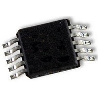
AD8592ARMZ Analog Devices Inc, AD8592ARMZ Datasheet - Page 8

AD8592ARMZ
Manufacturer Part Number
AD8592ARMZ
Description
OP AMP, +SHUTDOWN RRI/O, SMD, 8592
Manufacturer
Analog Devices Inc
Datasheet
1.AD8592ARMZ.pdf
(15 pages)
Specifications of AD8592ARMZ
Op Amp Type
Low Input Bias
No. Of Amplifiers
2
Bandwidth
2.2MHz
Slew Rate
5V/µs
Supply Voltage Range
2.5V To 6V
Amplifier Case Style
MSOP
No. Of Pins
10
Operating Temperature Range
-40°C To
Lead Free Status / RoHS Status
Lead free / RoHS Compliant
Available stocks
Company
Part Number
Manufacturer
Quantity
Price
Company:
Part Number:
AD8592ARMZ
Manufacturer:
Analog Devices Inc
Quantity:
31 712
Company:
Part Number:
AD8592ARMZ
Manufacturer:
AD
Quantity:
8 241
Part Number:
AD8592ARMZ
Manufacturer:
ADI/亚德诺
Quantity:
20 000
Company:
Part Number:
AD8592ARMZ-REEL
Manufacturer:
AD
Quantity:
1 538
Company:
Part Number:
AD8592ARMZ-REEL
Manufacturer:
Microsemi
Quantity:
1 538
Part Number:
AD8592ARMZ-REEL
Manufacturer:
ADI/亚德诺
Quantity:
20 000
Company:
Part Number:
AD8592ARMZ-REEL7
Manufacturer:
TOREX
Quantity:
800
AD8591/AD8592/AD8594
AD8591/AD8592/AD8594 APPLICATION SECTION
Theory of Operation
The AD859x family of amplifiers are all CMOS, high output drive,
rail-to-rail input and output single supply amplifiers designed for
low cost and high output current drive. The parts include a power
saving shutdown function making the AD8591/AD8592/AD8594
op amps ideal for portable multimedia and telecom applications.
Figure 29 shows the simplified schematic for an AD8591/AD8592/
AD8594 amplifier. Two input differential pairs, consisting of an
n-channel pair (M1-M2) and a p-channel pair (M3-M4), provide
a rail-to-rail input common-mode range. The outputs of the input
differential pairs are combined in a compound folded-cascode
stage, which drives the input to a second differential pair gain
stage. The outputs of the second gain stage provide the gate volt-
age drive to the rail-to-rail output stage.
The rail-to-rail output stage consists of M15 and M16, which are
configured in a complementary common-source configuration.
As with any rail-to-rail output amplifier, the gain of the output
stage, and thus the open-loop gain of the amplifier, is dependent
on the load resistance. Also, the maximum output voltage swing
is directly proportional to the load current. The difference be-
tween the maximum output voltage to the supply rails, known as
the dropout voltage, is determined by the AD8591/AD8592/
AD8594 output transistors’ on-channel resistance. The output
dropout voltage is given in Figure 1 and Figure 2.
Input Voltage Protection
Although not shown on the simplified schematic, ESD protec-
tion diodes are connected from each input to each power supply
rail. These diodes are normally reverse biased, but will turn on
if either input voltage exceeds either supply rail by more than
+0.6 V. Should this condition occur, the input current should
be limited to less than 5 mA. This can be done by placing a
resistor in series with the input(s). The minimum resistor value
should be:
IN–
SD
Figure 29. AD8591/AD8592/AD8594 Simplified Schematic
IN+
INV
R
M1
IN
50 A
INV
M3
V
IN MAX
5
,
mA
*
*
50 A
M4
V
M337
M2
M340
B3
V
B2
100 A
M5
M6
M7
*
V+
M8
*NOTE: ALL CURRENT SOURCES GO
V–
*
100 A
TO 0 A IN SHUTDOWN MODE
M9
M10
20 A
M12
M11
M13
*
M14
20 A
*
M30
M15
M16
M31
OUT
(1)
–8–
Output Phase Reversal
The AD8591/AD8592/AD8594 are immune to output voltage
phase reversal with an input voltage within the supply voltages
of the device. However, if either of the device’s inputs exceeds
+0.6 V outside of the supply rails, the output could exhibit
phase reversal. This is due to the ESD protection diodes be-
coming forward biased, thus causing the polarity of the input
terminals of the device to switch.
The technique recommended in the Input Overvoltage Protection
section should be applied in applications where the possibility of
input voltages exceeding the supply voltages exists.
Output Short Circuit Protection
To achieve high output current drive and rail-to-rail performance,
the outputs of the AD859x family do not have internal short cir-
cuit protection circuitry. Although these amplifiers are designed to
sink or source as much as 250 mA of output current, shorting the
output directly to the positive supply could damage or destroy the
device. To protect the output stage, the maximum output current
should be limited to 250 mA.
By placing a resistor in series with the output of the amplifier as
shown in Figure 30, the output current can be limited. The
minimum value for R
For a +5 V single supply application, R
Because R
tradeoff in using R
under heavy output current loads. R
tive output impedance of the amplifier to R
the output impedance of the device.
Power Dissipation
Although the AD859x family of amplifiers are able to provide
load currents of up to 250 mA, proper attention should be
given to not exceeding the maximum junction temperature for
the device. The equation for finding the junction temperature is
given as:
Where T
T
R
J
X
Figure 30. Output Short Circuit Protection
P
T
X
JA
DISS
J
A
P
= AD859x junction temperature
250
is inside the feedback loop, V
DISS
= The ambient temperature of the circuit
= AD859x junction-to-ambient thermal resistance
V
= AD859x power dissipation
of the package; and
V
SY
IN
mA
X
is a slight reduction in output voltage swing
J
A
X
can be found from Equation 2.
AD8592
T
+5V
A
20
R
X
X
will also increase the effec-
X
should be at least 20 .
OUT
O
V
+ R
is not affected. The
OUT
X
, where R
REV. A
O
is
(2)
(3)


