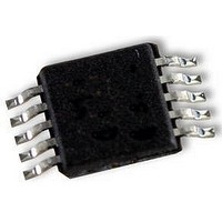
AD8592ARMZ Analog Devices Inc, AD8592ARMZ Datasheet - Page 4

AD8592ARMZ
Manufacturer Part Number
AD8592ARMZ
Description
OP AMP, +SHUTDOWN RRI/O, SMD, 8592
Manufacturer
Analog Devices Inc
Datasheet
1.AD8592ARMZ.pdf
(15 pages)
Specifications of AD8592ARMZ
Op Amp Type
Low Input Bias
No. Of Amplifiers
2
Bandwidth
2.2MHz
Slew Rate
5V/µs
Supply Voltage Range
2.5V To 6V
Amplifier Case Style
MSOP
No. Of Pins
10
Operating Temperature Range
-40°C To
Lead Free Status / RoHS Status
Lead free / RoHS Compliant
Available stocks
Company
Part Number
Manufacturer
Quantity
Price
Company:
Part Number:
AD8592ARMZ
Manufacturer:
Analog Devices Inc
Quantity:
31 712
Company:
Part Number:
AD8592ARMZ
Manufacturer:
AD
Quantity:
8 241
Part Number:
AD8592ARMZ
Manufacturer:
ADI/亚德诺
Quantity:
20 000
Company:
Part Number:
AD8592ARMZ-REEL
Manufacturer:
AD
Quantity:
1 538
Company:
Part Number:
AD8592ARMZ-REEL
Manufacturer:
Microsemi
Quantity:
1 538
Part Number:
AD8592ARMZ-REEL
Manufacturer:
ADI/亚德诺
Quantity:
20 000
Company:
Part Number:
AD8592ARMZ-REEL7
Manufacturer:
TOREX
Quantity:
800
Typical Performance Characteristics
AD8591/AD8592/AD8594
ABSOLUTE MAXIMUM RATINGS
Supply Voltage . . . . . . . . . . . . . . . . . . . . . . . . . . . . . . . . . +6 V
Input Voltage . . . . . . . . . . . . . . . . . . . . . . . . . . . . . GND to V
Differential Input Voltage . . . . . . . . . . . . . . . . . . . . . . . . 6 V
Output Short Circuit
Storage Temperature Range
Operating Temperature Range
Junction Temperature Range
Lead Temperature Range (Soldering, 60 sec) . . . . . . . +300 C
NOTES
1
2
CAUTION
ESD (electrostatic discharge) sensitive device. Electrostatic charges as high as 4000 V readily
accumulate on the human body and test equipment and can discharge without detection. Although
the AD8591/AD8592/AD8594 features proprietary ESD protection circuitry, permanent damage
may occur on devices subjected to high energy electrostatic discharges. Therefore, proper ESD
precautions are recommended to avoid performance degradation or loss of functionality.
Stresses above those listed under Absolute Maximum Ratings may cause perma-
For supplies less than 5 V the differential input voltage is limited to the supplies.
nent damage to the device. This is a stress rating only; functional operation of the
device at these or any other conditions above those listed in the operational sections
of this specification is not implied. Exposure to absolute maximum rating condi-
tions for extended periods may affect device reliability.
Figure 1. Output Voltage to Supply
Rail vs. Load Current
Duration to GND
R, RT, RM, RU Packages . . . . . . . . . . . . –65 C to +150 C
AD8591/AD8592/AD8594 . . . . . . . . . . . . –40 C to +85 C
R, RT, RM, RU Packages . . . . . . . . . . . . –65 C to +150 C
100
0.1
1k
10
1
0.01
V
T
A
S
= +2.7V
= +25 C
0.1
SOURCE
LOAD CURRENT – mA
1
2
. . . . . . . . . . . . Observe Derating Curves
10
SINK
100
1k
1
Figure 2. Output Voltage to Supply
Rail vs. Load Current
10k
100
0.1
1k
10
1
0.01
V
T
A
S
= +5V
= +25 C
0.1
LOAD CURRENT – mA
S
SOURCE
–4–
1
Package Type
6-Lead SOT-23 (RT)
10-Lead SOIC (RM)
16-Lead SOIC (R)
16-Lead TSSOP (RU)
NOTE
1
Model
AD8591ART –40 C to +85 C
AD8592ARM –40 C to +85 C
AD8594AR
AD8594ARU –40 C to +85 C
for surface mount packages.
JA
10
SINK
is specified for worst case conditions, i.e.,
100
1k
Temperature
Range
–40 C to +85 C
ORDERING GUIDE
0.90
0.85
0.80
0.75
0.70
0.65
0.60
0.55
0.50
Figure 3. Supply Current per
Amplifier vs. Temperature
40
230
200
120
180
JA
1
WARNING!
20
Package
Description
6-Lead SOT-23
10-Lead SOIC
16-Lead SOIC
16-Lead TSSOP
JA
TEMPERATURE – C
0
is specified for device in socket
92
44
36
35
20
JC
ESD SENSITIVE DEVICE
40
V
S
= +2.7V
V
60
S
Units
C/W
C/W
C/W
C/W
= +5V
Package
Option
RT-6
RM-10
R-16A
RU-16
80
REV. A
100


