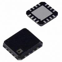
ADG1611BCPZ-REEL7 Analog Devices Inc, ADG1611BCPZ-REEL7 Datasheet - Page 9

ADG1611BCPZ-REEL7
Manufacturer Part Number
ADG1611BCPZ-REEL7
Description
IC, ANALOG SWITCH, QUAD, SPST, LFCSP-16
Manufacturer
Analog Devices Inc
Type
Analog Switchr
Datasheet
1.ADG1612BCPZ-REEL7.pdf
(16 pages)
Specifications of ADG1611BCPZ-REEL7
Analog Switch Type
SPST
No. Of Channels
4
Bandwidth
42MHz
On State Resistance Max
1ohm
Turn Off Time
105ns
Turn On Time
165ns
Supply Voltage Range
3.3V To 16V
Design Resources
Low Cost Programmable Gain Instrumentation Amplifier Circuit Using ADG1611 and AD620 (CN0146)
Function
Switch
Circuit
4 x SPST - NO
On-state Resistance
1.2 Ohm
Voltage Supply Source
Single, Dual Supply
Voltage - Supply, Single/dual (±)
3.3 V ~ 16 V, ±3.3 V ~ 8 V
Current - Supply
1µA
Operating Temperature
-40°C ~ 85°C
Mounting Type
Surface Mount
Package / Case
16-VQFN, CSP Exposed Pad
Multiplexer Configuration
Quad SPST
Number Of Inputs
4
Number Of Outputs
4
Number Of Channels
4
Power Supply Requirement
Single/Dual
Single Supply Voltage (min)
3.3V
Single Supply Voltage (typ)
5/9/12/15V
Single Supply Voltage (max)
16V
Dual Supply Voltage (typ)
±5V
Dual Supply Voltage (max)
±8V
Mounting
Surface Mount
Pin Count
16
Operating Temp Range
-40C to 125C
Operating Temperature Classification
Automotive
Rohs Compliant
Yes
Lead Free Status / RoHS Status
Lead free / RoHS Compliant
Lead Free Status / RoHS Status
Lead free / RoHS Compliant, Lead free / RoHS Compliant
Available stocks
Company
Part Number
Manufacturer
Quantity
Price
Company:
Part Number:
ADG1611BCPZ-REEL7
Manufacturer:
NXP
Quantity:
491
PIN CONFIGURATIONS AND FUNCTION DESCRIPTIONS
Table 7. Pin Function Descriptions
16-Lead TSSOP
1
2
3
4
5
6
7
8
9
10
11
12
13
14
15
16
N/A
Table 8. ADG1611/ADG1612 Truth Table
ADG1611 INx
0
1
Table 9. ADG1613 Truth Table
Logic (INx)
0
1
Figure 4. 16-Lead TSSOP Pin Configuration
GND
NC = NO CONNECT
V
IN1
IN4
Pin No.
D1
D4
S1
S4
SS
1
2
3
4
5
6
7
8
16-Lead LFCSP
15
16
1
2
3
4
5
6
7
8
9
10
11
12
13
14
17 (EPAD)
(Not to Scale)
ADG1612/
ADG1611/
ADG1613
TOP VIEW
16
15
14
13
12
11
10
9
IN2
D2
S2
V
NC
S3
D3
IN3
DD
ADG1612 INx
1
0
Switch 1, Switch 4
Off
On
Mnemonic
IN1
D1
S1
V
GND
S4
D4
IN4
IN3
D3
S3
NC
V
S2
D2
IN2
EP (EPAD)
SS
DD
Rev. A | Page 9 of 16
Description
Logic Control Input.
Drain Terminal. This pin can be an input or output.
Source Terminal. This pin can be an input or output.
Most Negative Power Supply Potential.
Ground (0 V) Reference.
Source Terminal. This pin can be an input or output.
Drain Terminal. This pin can be an input or output.
Logic Control Input.
Logic Control Input.
Drain Terminal. This pin can be an input or output.
Source Terminal. This pin can be an input or output.
No Connection.
Most Positive Power Supply Potential.
Source Terminal. This pin can be an input or output.
Drain Terminal. This pin can be an input or output.
Logic Control Input.
Exposed Pad. Tied to substrate, V
NOTES
1. NC = NO CONNECT.
2. EXPOSED PAD TIED TO SUBSTRATE, V
Figure 5. 16-Lead LFCSP Pin Configuration
GND
V
S1
S4
SS
ADG1611/ADG1612/ADG1613
1
2
3
4
Switch Condition
On
Off
Switch 2, Switch 3
On
Off
(Not to Scale)
ADG1611/
ADG1612/
ADG1613
TOP VIEW
PIN 1
INDICATOR
SS
.
12 S2
11 V
10 NC
9 S3
DD
SS
.


