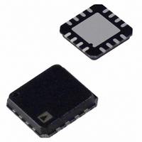
ADG1611BCPZ-REEL7 Analog Devices Inc, ADG1611BCPZ-REEL7 Datasheet - Page 8

ADG1611BCPZ-REEL7
Manufacturer Part Number
ADG1611BCPZ-REEL7
Description
IC, ANALOG SWITCH, QUAD, SPST, LFCSP-16
Manufacturer
Analog Devices Inc
Type
Analog Switchr
Datasheet
1.ADG1612BCPZ-REEL7.pdf
(16 pages)
Specifications of ADG1611BCPZ-REEL7
Analog Switch Type
SPST
No. Of Channels
4
Bandwidth
42MHz
On State Resistance Max
1ohm
Turn Off Time
105ns
Turn On Time
165ns
Supply Voltage Range
3.3V To 16V
Design Resources
Low Cost Programmable Gain Instrumentation Amplifier Circuit Using ADG1611 and AD620 (CN0146)
Function
Switch
Circuit
4 x SPST - NO
On-state Resistance
1.2 Ohm
Voltage Supply Source
Single, Dual Supply
Voltage - Supply, Single/dual (±)
3.3 V ~ 16 V, ±3.3 V ~ 8 V
Current - Supply
1µA
Operating Temperature
-40°C ~ 85°C
Mounting Type
Surface Mount
Package / Case
16-VQFN, CSP Exposed Pad
Multiplexer Configuration
Quad SPST
Number Of Inputs
4
Number Of Outputs
4
Number Of Channels
4
Power Supply Requirement
Single/Dual
Single Supply Voltage (min)
3.3V
Single Supply Voltage (typ)
5/9/12/15V
Single Supply Voltage (max)
16V
Dual Supply Voltage (typ)
±5V
Dual Supply Voltage (max)
±8V
Mounting
Surface Mount
Pin Count
16
Operating Temp Range
-40C to 125C
Operating Temperature Classification
Automotive
Rohs Compliant
Yes
Lead Free Status / RoHS Status
Lead free / RoHS Compliant
Lead Free Status / RoHS Status
Lead free / RoHS Compliant, Lead free / RoHS Compliant
Available stocks
Company
Part Number
Manufacturer
Quantity
Price
Company:
Part Number:
ADG1611BCPZ-REEL7
Manufacturer:
NXP
Quantity:
491
ADG1611/ADG1612/ADG1613
ABSOLUTE MAXIMUM RATINGS
T
Table 6.
Parameter
V
V
V
Analog Inputs
Digital Inputs
Peak Current, S or D
Continuous Current, S or D
Operating Temperature Range
Storage Temperature Range
Junction Temperature
16-Lead TSSOP, θ
16-Lead LFCSP, θ
Reflow Soldering Peak
1
2
Overvoltages at IN, S, or D are clamped by internal diodes. Current should be
limited to the maximum ratings given.
See Table 5.
DD
DD
SS
A
Industrial (Y Version)
Impedance (2-Layer Board)
Impedance (4-Layer Board)
Temperature, Pb free
= 25°C, unless otherwise noted.
to GND
to V
to GND
SS
1
1
JA
JA
Thermal
Thermal
2
Rating
18 V
−0.3 V to +18 V
+0.3 V to −18 V
V
30 mA, whichever occurs first
GND − 0.3 V to V
30 mA, whichever occurs first
630 mA (pulsed at 1 ms,
10% duty-cycle maximum)
Data + 15%
−40°C to +125°C
−65°C to +150°C
150°C
150.4°C/W
48.7°C/W
260°C
SS
− 0.3 V to V
DD
DD
+ 0.3 V or
+ 0.3 V or
Rev. A | Page 8 of 16
Stresses above those listed under Absolute Maximum Ratings
may cause permanent damage to the device. This is a stress
rating only; functional operation of the device at these or any
other conditions above those indicated in the operational
section of this specification is not implied. Exposure to absolute
maximum rating conditions for extended periods may affect
device reliability.
ESD CAUTION


