AD630AD Analog Devices Inc, AD630AD Datasheet - Page 2
AD630AD
Manufacturer Part Number
AD630AD
Description
MODULATOR / DEMODULATOR IC
Manufacturer
Analog Devices Inc
Datasheet
1.AD630JNZ.pdf
(12 pages)
Specifications of AD630AD
Rf Type
Balanced
Supply Voltage Range
± 5V To �� 16.5V
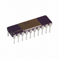
Rf Ic Case Style
DIP
No. Of Pins
20
Operating Temperature Range
-25°C To +85°C
Peak Reflow Compatible (260 C)
No
Leaded Process Compatible
No
Rohs Status
RoHS non-compliant
Function
Modulator/Demodulator
Frequency
2MHz
Package / Case
20-CDIP (0.300", 7.62mm)
Mounting Type
Through Hole
Rohs Compliant
No
Lead Free Status / RoHS Status
Contains lead / RoHS non-compliant
Available stocks
Company
Part Number
Manufacturer
Quantity
Price

Part Number:
AD630AD
Manufacturer:
ADI/亚德诺
Quantity:
20 000


Model
GAIN
CHANNEL INPUTS
COMPARATOR
DYNAMIC PERFORMANCE
OPERATING CHARACTERISTICS
OUTPUT VOLTAGE, @ R
TEMPERATURE RANGES
NOTES
1
2
3
Specifications subject to change without notice.
AD630–SPECIFICATIONS
If one terminal of each differential channel or comparator input is kept within these limits the other terminal may be taken to the positive supply.
I
Pin 12 Open. Slew rate with Pin 12 and Pin 13 shorted is typically 35 V/ µs.
SINK
Open-Loop Gain
± 1, ± 2 Closed-Loop Gain Error
Closed-Loop Gain Match
Closed-Loop Gain Drift
V
Input Offset Voltage
Input Offset Voltage
Input Bias Current
Input Offset Current
Channel Separation @ 10 kHz
V
Switching Window
Switching Window
Input Bias Current
Response Time (–5 mV to +5 mV Step)
Channel Status
Unity Gain Bandwidth
Slew Rate
Settling Time to 0.1% (20 V Step)
Common-Mode Rejection
Power Supply Rejection
Supply Voltage Range
Supply Current
T
Output Short-Circuit Current
Rated Performance–N Package
Rated
IN
IN
MIN
T
T
I
Pull-Up Voltage
@ V
SINK
Operational Limit
Operational Limit
MIN
MIN
to T
Performance–D Package
OL
@ V
to T
to T
3
= (–V
MAX
OL
MAX
MAX
= –V
S
+ 1); V is typically 4 mA.
S
+ 0.4 V
1
1
L
= 2 kΩ
2
Min
90
(–V
(–V
1.6
85
90
± 5
± 10
0
–25
S
S
+ 4 V) to (+V
+ 3 V) to (+V
AD630J/AD630A
Typ
45
3
4
110
0.1
0.1
2
100
10
100
100
200
2
105
110
25
(@ 25 C and V
Max
500
800
300
50
± 1.5
± 2.0
300
(–V
± 16.5
5
70
+85
S
S
S
– 1 V)
– 1.5 V)
+ 33 V)
Min
100
(–V
(–V
1.6
90
90
± 5
± 10
0
–25
–2–
S
= 15 V, unless otherwise noted.)
S
S
+ 4 V) to (+V
+ 3 V) to (+V
AD630K/AD630B
Typ
120
2
100
10
100
100
200
2
45
3
110
110
4
25
S
S
Max
0.05
0.05
100
160
300
50
± 1.5
± 2.0
300
(–V
± 16.5
5
70
+85
– 1 V)
– 1.5 V)
S
+ 33 V)
Min
(–V
(–V
1.6
± 5
± 10
90
90
90
–55
S
S
+ 4 V) to (+V
+ 3 V) to (+V
Typ
110
0.1
0.1
2
100
10
100
100
200
2
45
3
110
110
4
25
N/A
AD630S
Max
500
1000
300
50
± 1.5
± 2.5
300
(–V
± 16.5
5
+125
S
S
– 1 V)
– 1.3 V)
S
+ 33 V)
Unit
dB
%
%
ppm/°C
V
µV
µV
nA
nA
dB
V
mV
mV
nA
ns
mA
V
MHz
V/µs
µs
dB
dB
V
mA
V
mA
°C
°C
REV. E
Related parts for AD630AD
Image
Part Number
Description
Manufacturer
Datasheet
Request
R

Part Number:
Description:
±1.7g Dual-Axis IMEMS Accelerometer Evaluation Board
Manufacturer:
Analog Devices Inc
Datasheet:

Part Number:
Description:
Inertial Sensor Evaluation System
Manufacturer:
Analog Devices Inc
Datasheet:
Part Number:
Description:
Manufacturer:
Analog Devices Inc
Datasheet:
Part Number:
Description:
Manufacturer:
Analog Devices Inc
Datasheet:
Part Number:
Description:
Manufacturer:
Analog Devices Inc
Datasheet:
Part Number:
Description:
Manufacturer:
Analog Devices Inc
Datasheet:
Part Number:
Description:
Manufacturer:
Analog Devices Inc
Datasheet:
Part Number:
Description:
Manufacturer:
Analog Devices Inc
Datasheet:
Part Number:
Description:
Manufacturer:
Analog Devices Inc
Datasheet:
Part Number:
Description:
Manufacturer:
Analog Devices Inc
Datasheet:
Part Number:
Description:
Manufacturer:
Analog Devices Inc
Datasheet:
Part Number:
Description:
Manufacturer:
Analog Devices Inc
Datasheet:
Part Number:
Description:
Manufacturer:
Analog Devices Inc
Datasheet: