LM5642MTC National Semiconductor, LM5642MTC Datasheet - Page 3
LM5642MTC
Manufacturer Part Number
LM5642MTC
Description
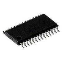
IC, DUAL SYNC BUCK CONVERTER, 28-TSSOP
Manufacturer
National Semiconductor
Datasheet
1.LM5642MTCNOPB.pdf
(28 pages)
Specifications of LM5642MTC
Primary Input Voltage
36V
No. Of Outputs
2
Output Voltage
32.4V
Output Current
20A
No. Of Pins
28
Operating Temperature Range
-40°C To +125°C
Power Dissipation Pd
1.1W
Lead Free Status / RoHS Status
Contains lead / RoHS non-compliant
Available stocks
Company
Part Number
Manufacturer
Quantity
Price

Part Number:
LM5642MTC
Manufacturer:
NS/国半
Quantity:
20 000
Part Number:
LM5642MTC/LM5642XMT
Manufacturer:
NS/国半
Quantity:
20 000
Company:
Part Number:
LM5642MTC/NOPB
Manufacturer:
NS
Quantity:
217
Part Number:
LM5642MTCX
Manufacturer:
NS/国半
Quantity:
20 000
Company:
Part Number:
LM5642MTCX/NOPB
Manufacturer:
TI
Quantity:
7 966


goes into shut down mode. Adding a capacitor to this pin pro-
vides a soft-start feature that minimizes inrush current and
output voltage overshoot.
ON/SS2 (Pin 10): Channel 2 enable pin. See the description
for Pin 9, ON/SS1. May be connected to ON/SS1 for simul-
taneous startup or for parallel operation.
FB2 (Pin 11): Feedback input for channel 2. Connect to
VOUT through a voltage divider to set the Channel 2 output
voltage.
COMP2 (Pin 12): Compensation pin for Channel 2. This is
the output of the internal transconductance error amplifier.
The loop compensation network should be connected be-
tween this pin and the signal ground SGND (Pin 8).
ILIM2 (Pin 13): Current limit threshold setting for Channel 2.
See ILIM1 (Pin 2).
KS2 (Pin 14): The positive (+) Kelvin sense for the internal
current sense amplifier of Channel 2. See KS1 (Pin 1).
RSNS2 (Pin 15): The negative (-) Kelvin sense for the internal
current sense amplifier of Channel 2. Connect this pin to the
low side of the current sense resistor that is placed between
VIN and the drain of the top MOSFET. When the Rds of the
top MOSFET is used for current sensing, connect this pin to
the source of the top MOSFET. Always use a separate trace
to form a Kelvin connection to this pin.
SW2 (Pin 16): Switch-node connection for Channel 2, which
is connected to the source of the top MOSFET of Channel 2.
It serves as the negative supply rail for the top-side gate driv-
er, HDRV2.
HDRV2 (Pin 17): Top-side gate-drive output for Channel 2.
HDRV is a floating drive output that rides on the correspond-
ing switching-node voltage.
CBOOT2 (Pin 18): Bootstrap capacitor connection. It serves
as the positive supply rail for the Channel 2 top-side gate
3
drive. Connect this pin to VDD2 (Pin 19) through a diode, and
connect the low side of the bootstrap capacitor to SW2
(Pin16).
VDD2 (Pin 19): The supply rail for the Channel 2 low-side
gate drive. Connected to VLIN5 (Pin 7) through a 4.7Ω resis-
tor and bypassed to power ground with a ceramic capacitor
of at least 1µF. Tie this pin to VDD1 (Pin 24).
LDRV2 (Pin 20): Low-side gate-drive output for Channel 2.
PGND (Pin 21): The power ground connection for both chan-
nels. Connect to the ground rail of the system.
VIN (Pin 22): The power input pin for the chip. Connect to the
positive (+) input rail of the system. This pin must be con-
nected to the same voltage rail as the top FET drain (or the
current sense resistor when used).
LDRV1 (Pin 23): Low-side gate-drive output for Channel 1.
VDD1 (Pin 24): The supply rail for Channel 1 low-side gate
drive. Tie this pin to VDD2 (Pin 19).
CBOOT1 (Pin 25): : Bootstrap capacitor connection. This pin
serves as the positive supply rail for the Channel 1 top-side
gate drive. See CBOOT2 (Pin 18).
HDRV1 (Pin 26): Top-side gate-drive output for Channel 1.
See HDRV2 (Pin 17).
SW1 (Pin 27): Switch-node connection for Channel 1. See
SW2 (Pin16).
RSNS1 (Pin 28): The negative (-) Kelvin sense for the internal
current sense amplifier of Channel 1. See RSNS2 (Pin 15).
PGND (DAP): The power ground connection for both chan-
nels. Connect to the ground rail of the system. Use of multiple
vias to internal ground plane or GND layer helps to dissipate
heat generated by output power.
www.national.com
Related parts for LM5642MTC
Image
Part Number
Description
Manufacturer
Datasheet
Request
R

Part Number:
Description:
National Semiconductor [8-Bit D/A Converter]
Manufacturer:
National Semiconductor
Datasheet:
Part Number:
Description:
National Semiconductor [Media Coprocessor]
Manufacturer:
National Semiconductor
Datasheet:
Part Number:
Description:
Digitally Controlled Tone and Volume Circuit with Stereo Audio Power Amplifier, Microphone Preamp Stage and National 3D Sound
Manufacturer:
National Semiconductor
Datasheet:
Part Number:
Description:
Digitally Controlled Tone and Volume Circuit with Stereo Audio Power Amplifier, Microphone Preamp Stage and National 3D Sound
Manufacturer:
National Semiconductor
Datasheet:
Part Number:
Description:
AC97 Rev 2 Codec with Sample Rate Conversion and National 3D Sound
Manufacturer:
National Semiconductor
Part Number:
Description:
Manufacturer:
National Semiconductor
Datasheet:
Part Number:
Description:
Manufacturer:
National Semiconductor
Datasheet:
Part Number:
Description:
General Purpose, Low Voltage, Low Power, Rail-to-Rail Output Operational Amplifiers
Manufacturer:
National Semiconductor
Datasheet:
Part Number:
Description:
8-bit 20 MSPS flash A/D converter.
Manufacturer:
National Semiconductor
Datasheet:
Part Number:
Description:
Low Noise Quad Operational Amplifier
Manufacturer:
National Semiconductor
Datasheet:
Part Number:
Description:
Quad Differential Line Receivers
Manufacturer:
National Semiconductor
Datasheet:
Part Number:
Description:
Quad High Speed Trapezoidal? Bus Transceiver
Manufacturer:
National Semiconductor
Datasheet:
Part Number:
Description:
Dual Line Receiver
Manufacturer:
National Semiconductor
Datasheet:
Part Number:
Description:
TTL to 10k ECL Level Translator with Latch
Manufacturer:
National Semiconductor
Datasheet: